This thread has been locked.

If you have a related question, please click the "Ask a related question" button in the top right corner. The newly created question will be automatically linked to this question.

TPS25983: TPS25983 Slew Rate

Part Number: TPS25983
Other Parts Discussed in Thread: , TPS1685

Tool/software:

Hi,

I evaluate the Inrush Current Control of the efuse TPS25983 with  the TPS25983EVM board, I want ot use it to limit the inrush current with a large output capacitor.  

I test it following the test setup and procedure outlined in SLUUCW7 document, §2.3.1 Hot-Plug Test: 

Jumper J12 in 3-4, J4 open, J6 in 1-2, J7 in 2-3, J8 install, J9 in 3-4, J10 in 5-6, J11 open, J13 install

Vin =12V and teh current limit is 15A

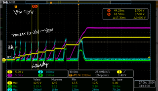
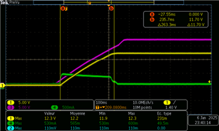
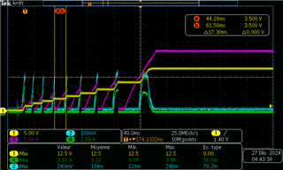
When I test with a output capacitance of 2000 uF, I measure with oscilloscope a Slew Rate close to  0,5V/ms  :  Ch1 (yellow)= Vout , CH2= IMON, CH3= gate & CH4=Iin 

When I test with a output capacitance of 6800 uF, I don't understand its operating, it retries 8 times to charge the output capacitance  : Ch1 = Vout , CH2= IMON, CH3= gate & CH4=Iin 


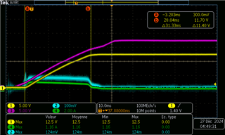
During the charge, the vin voltage is above UVLO, 10,87V.

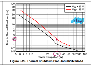
I was thinking to see a charge in one time only with a SR close  to 0,5V/ms thanks the Ilimit is 18A, can you explain me what i didn't understand .

Thanks,

Jerome

  • Hi Jerome,

    Thank you for patience. I was ooo earlier. 

    It looks like the device is performing thermal shutdown and then auto-retry during the startup test with higher capacitor. If you check the power dissipation (annotated waveform attached), the device performs the TSD to keep the SOA of FET.

    Can you also try with lower slew rate? But your application require 0.5V/ms startup slew rate. We have a calculator which can tell if the TSD will happen during startup or glitch free startup is possible.

    Best regards,
    Arush

  • Hi,

    I used the TPS25983 design calculator tool, and the calculated value of capacitor at dVdT pin at is 76nF (SR=0,06V/ms).

    So I updated C14 = 68nF and with jumper J12 in 1-2 & 3-4, CdVdT is 78nF =>  now, the large output capacitor is charged one time with a inrush current <500mA. (Ch1 = Vout , CH3= gate & CH4=Iin)

    The behavior is good! 

    thanks,

    jerome

  • The input voltage of my product will be 9V to 30V, so I plan to use the TPS1685 component instead of the TPS25983 (Vin MAX =26V).

    Its  status is preproduction, can you tell me more.

    The TPS1685  doesn't include the reverse input polarity protection, do you a have another reference to suggest me with it ?

  • Hi Jerome,

    Good to hear that the issue is resolved. You can check the advanced information on TPS1685 for more information.

    https://www.ti.com/lit/ds/symlink/tps1685.pdf?ts=1736246789047&ref_url=https%253A%252F%252Fwww.ti.com%252Fproduct%252FTPS1685

    Also if you need input side reverse polarity protection, you can use a Schottky diode between the device GND and the system GND to implement RPP with any eFuse. 

    Best Regards,
    Arush