This thread has been locked.

If you have a related question, please click the "Ask a related question" button in the top right corner. The newly created question will be automatically linked to this question.

TPS54360B: IC heating up rapidly when applying 60V to the input

Part Number: TPS54360B

Tool/software:

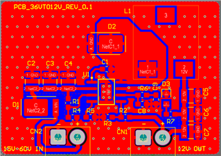
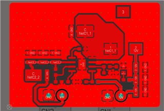
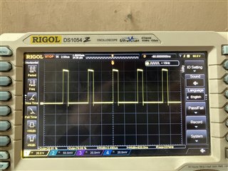
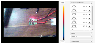
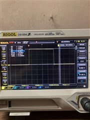
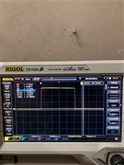
I had designed the buck converter with output voltage of 12V @3.5A. The heating was normal when the input voltage was around 17V to 36V but when applying 60V to the input the chip started heating up rapidly, the load current was about 2.33A @12V during the testing. But no output voltage drop were observed during the testing. The chip temperature rose to about >70 degC. What might be the issue? Is it normal for the chip to rise to such a high temperature during high voltage inputs? Or better thermal management required during high voltage application? I have attached the schematic and layout for your reference.buckconverter.pdf

  • Hello Tenzing

    Thanks for writing to us!

    I will get back to you on this tomorrow.  

    Regards

    Onkar Bhakare

  • Thanks. Sure please let me know the possible causes as soon as possible.

  • Hello Tenzing

    At higher Vin, switching losses would increase leading to higher dissipation in the device. You need provide sufficient copper area for heat dissipation to keep temperature within limits. Could you please share bottom layer picture also to see how power PAD is connected to it.

    Moreover, you can use QuickStart of the device to compare the dissipation. Kindly fill the quickstart and share it over this thread.

    Thank you

    Regards

    Onkar Bhakare

  • Hello,
    I couldnot find the quick start form can you please share it to me.
    I have attached the top and bottom layer of the layout. The copper thickness is 1oz.

  • Hello Tenzing 

    Thanks for sharing the layout images. I'll have look on it.

    For quickstart you can use this link - SLVC452 Calculation tool | TI.com

    For most of our devices it is located under 'Design and development" section of product page.

    Thank you

    Regards

    Onkar Bhakare

  • Hello Onkar,
    Thanks for the ink. I have shared yout the quick start file please have a look at it.

    6471.TPS54360-361FAMILY_CALC_TOOL_REVE.xls

  • Hello Tenzing

    Thanks for sharing the QuickStart!

    If you look at the power dissipation section of the calculator, you will see that the max power dissipation in the IC is 1.93 W, which is high and could trigger thermal shutdown if ambient temperature is high enough. 

    From a quick review your layout looks good. However, to gain a clearer understanding of the temperature rise and to assess whether the board area and vias are sufficient, I recommend referring to this application note - AN-2020 Thermal Design By Insight, Not Hindsight (Rev. C)

    You can also reduce switching frequency to ~400 kHz to reduce power dissipation, it would give you sufficient enough margin from hitting Tj_max of the IC. 

    Let me know if you have further questions. Kindly close the thread if you feel issue is resolved

    Thank you

    Regards

    Onkar Bhakare

  • hello Onkar,
    Thanks for the app note and your suggestion, I will reduce the switching frequency and let you know the test results.

  • Hi onkar,
    I tried reducing the frequency from 400-200KHz but only slight improvement was observed. At around 200KHz the converter was stable at 3.4A but the temperature of the IC reached around 80 degC at 25 degC ambient temperature. I think at higher ambient temperature the device will undergo thermal shutdown. Do you have any other options? Also i noticed one more issue when applying 60V input , the IC burned (at no load) but when reducing the rise time of the power supply there was no issue. Is there a way to increase the soft start time without the infulence of the switching frequency.

  • Hi Tenzing

    To get better idea of the issue could you please share following test results

    1. SW node waveform 
    2. Measured efficiency of the converter. Measure Vin right across the cap closest to IC

    How are measuring the temperature of the device? Could you please confirm the technique?

    Couple of points I missed earlier on layout, I didn't look aspects other than thermal

    1. Placement of diode, input cap and boot resistor is not optimal. SW node connection to boot capacitor can be taken from the other layer to make continuous connection of GND pad and GND connections of diode and input cap. Refer datasheet section 10.1 Layout Guidelines
    2. Output cap can also be arranged in the way shown in following example
    3. SW pour is quite large and can be optimized to improve EMI performance

    Thank you

    Regards

    Onkar

  • Hello Onkar,
    I have attached the SW node waveform and the temperatures, the temperatures were measured using thermal camera.
    measured points: 
    1:IC
    2: reverse protection diode
    3: Inductor
    4: catch diode
    5: board temperature (top)
    6: ambient
    Input voltage measured across the capacitor: 59.54V
    Input current: 0.742A
    Power: 44.17W
    Output voltage: 11.97V
    Current: 3.42
    Power: 40.93W
    efficiency: 92.6%
    Also thankyou very much for layout suggestions, I will improve it in my next iteration.
    Also in previous thread I asked about increasing the softstart time, is there any way to increase it? The chip blows off when connected directly to 60V at no load but when the input slowly rises to 60V then the chip doesn't blows off. 

  • Hi Tenzing

    Thanks for sharing the waveform. 

    I have listed my comment below,

    Also in previous thread I asked about increasing the softstart time, is there any way to increase it? The chip blows off when connected directly to 60V at no load but when the input slowly rises to 60V then the chip doesn't blows off. 
    1. This could be due hot plugging the device with 60V power supply. As you have long wire harness connecting to the input of the PCB, Input seen by the device could go higher than abs max rating result in damage of the device.
    2. If harness is longer in the real system, sufficient damping must be provided at the input to avoid potential failure. You can use elctrolytic capacitors at input.
    3. Looking at the peak of the SW waveform, operating voltage seems higher than 60V. Continous operation above operating voltage is not recommended. Additionally, SW ringing can make problem worse. To get better picture of this, could you please set, bandwidth of Ch1 to maximum and measure SW node voltage with shortest measuring loop.
    4. How does input profile in your application looks like? Is 60 V Vin a continuous operational condition or is it a momentary situation?  If it is an operational condition, then there isn't an enough margin to protect the device.
    5. Device has internal soft start and the time depends on the frequency setting. Moreover, increasing the soft start time won't help in this condition as it doesn't control the input.

    I hope this answers your question. Let me know if you need any clarification or further help.

    Thank you

    Regards

    Onkar


  • Hi Onkar,
    Thanks for the suggestions, i try to add a capacitor at the input and let you know the test results.
    I have also attached the waveforms as per your request. The peak was at 61.6V and the undershoot was 4.4V you can see in the waveform.
    And yes this device must operate continuously at around 58V, since the input source is 48V battery bank and the voltage will rise to about 57.6V when fully charged.
    please let me know if you need any other measurements to further find out the issue.
          

  • Hi Tenzing

    As I mentioned in earlier post, operating converter above its recommend Vin should be avoided. 

    you can also measure input voltage right across the close input cap to the IC. Let me know once results with electrolytic capacitor is available to you.

    Thank you

    Regards

    Onkar Bhakare