This thread has been locked.

If you have a related question, please click the "Ask a related question" button in the top right corner. The newly created question will be automatically linked to this question.

LM5122: Difficulties to startup dual phase boost converter

Part Number: LM5122

Tool/software:

Hello,

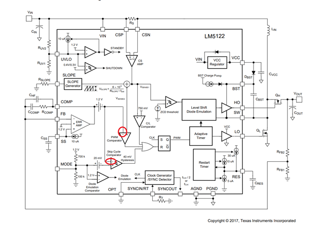
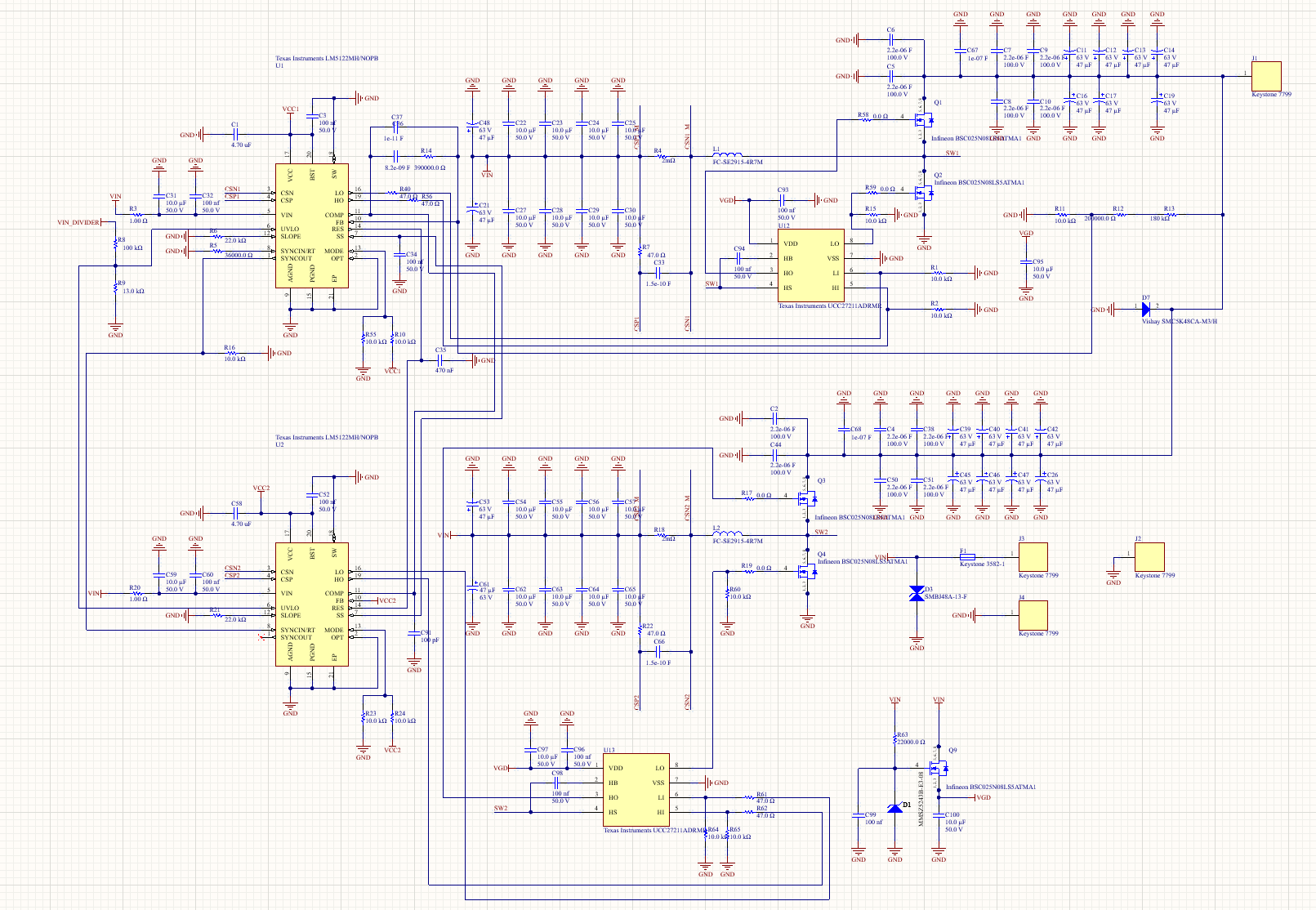
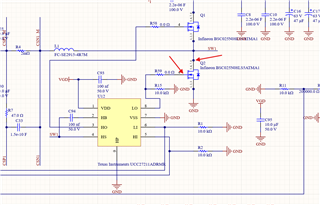
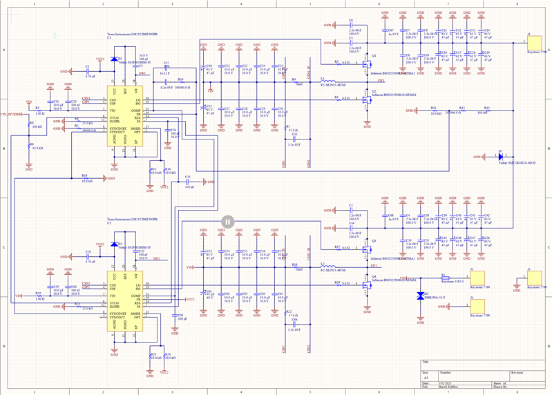
I am working on a 300W 12V to 48V boost converter, this is based on a 2phase boost converter based on the LM5122.

The schematic is shown below:

When only the master is stuffed, the converter starts properly.

However when the extra slave converter is added, there is a strange behavior visible.

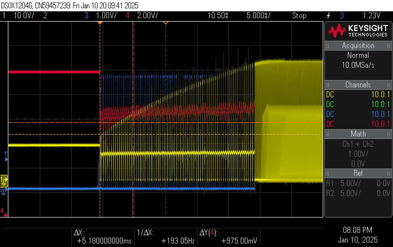
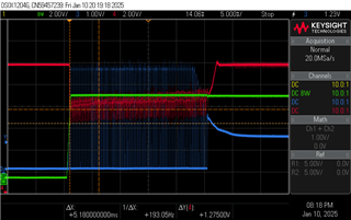
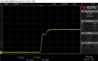
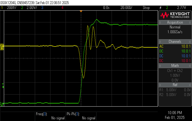
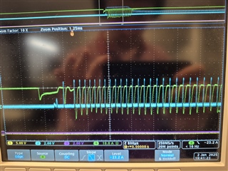
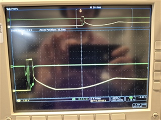
During startup of the converter or with a load, when the converter(s) start switching the output of the error amplifier starts rising very quickly ~1V/50us and commands a very high current from the inner current loop.

This results in a large voltage drop at the input, this voltage drop triggers the UVLO of the converter and is disabled and start up again.

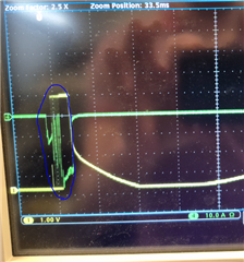
This is shown in the scope plot below, green is the input current and blue is the output of the error amplifier.

Normally such a steep response isn`t expected because the bandwidth of the error amplifier is quite slow, the slave error amplifier should be disabled because the FB is connected to VCC (output of internal LDO)

So i don`t see any situation where this behavior is possible.

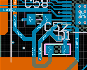
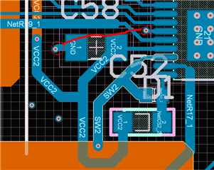
I double checked the schematic a couple of times but i can`t see where there could be a problem, i also tried different operation modes but the problem stays the same.

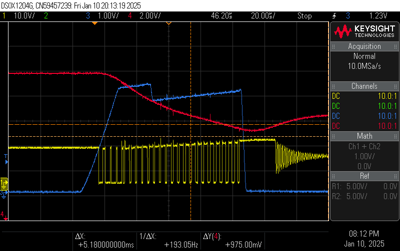
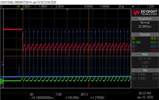
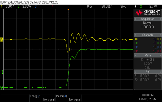
After doing some double checking and removing the slave controller, the problem is also visible with just the master controller.

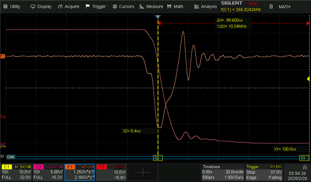
During startup there also unexpected transients visible on the ouput of the error amplifier (Yellow trace)

Kind Regards

Alexander

Kind Regards

Alexander

  • Hi Alex,

    Our engineer is out of office, and will return on the 7th of January. Please expect some delays in our response. 

    Best Regards,

    Feng

  • Hi Alex,

    Thank you very much for your patience.

    A 2mOhm sense resistor would set the current limit on each phase to 37.5A. This seems to be more than the input can supply and also more than the application requires in general (150W at each phase).

    Could you increase the sense resistance at both phases to 4mOhm? This should increase the system stability and reduce the current limit on each phase to 18.75A.

    Best regards,
    Niklas

  • Ok thanks for the feedback, i don`t have such sense resistors at the moment so it will takes some time to order.


    I was also wondering why the toggling of the error amplifier happens, i never seen such a toggling of the error amplifier, normally the response should be quite slow.

    Do you have ever seen such a behavior of the error amplifier?

  • Hi Alex,

    Thanks for the update.

    The FB pin (before the error amplifier) follows the output voltage, so the voltage loop is rather slow.
    The COMP pin (after the error amplifer) is also affected by the internal current sensing slope. The current loop reacts much faster than the voltage loop and directly affects the duty cycle.
    If a protection circuit triggers, such as UVLO, the COMP pin should be actively discharged, which can also result in a fast change of the COMP pin votlage.

    Best regards,
    Niklas

  • Hello Niklas,

    Thanks for the feedback, really appreciated!

    Yes indeed, the bandwidth of the error amplifier is quite slow due the RHP zero.

    I don`t fully understand why the COMP pin should be affected by the current sensing slope, i know the current loop is very fast and triggered when the sum of the sensed inductor and the slope compensation is greater then the command value by the slow voltage loop.

    But the COMP voltage is the input of the PWM comparator (and skip cycle) and shouldn`t be directly affected by the internal current sensing slope?

    Or is there still some other things that can affect the COMP voltage beside the error amplifier.

    Of course an high inductor current means a big charging current and rises the output voltage and counteracts itself, the commanded inductor current will be decreased by the outer voltage loop.


    Ok thanks, good to know there is an active discharge when an UVLO is detected.

    Still wondering how such a large increase of the error amplifier is possible?

    It`s like a large voltage step, and the error amplifier seems to be hitting a slew rate limit?, or is there something that can affect this voltage?

    Kind Regards

    Alexander

  • Hi Alex,

    Thanks for the clarification.
    Sorry that it took a while for me to fully understand the question.
    You are referring the the fast jumping up and down directly at the beginning on the waveform correct?

    I agree with you that this looks indeed strange.
    The COMP pin shoot up to ~4V, which would mean in theory that the device will switch with maximum duty cycle.
    Normally, the softstart is active to slowly ramp up the reference voltage of the error amplifier to avoid such strong inrush currents.
    If the SS cap is too small, the reference slope will go up faster than the actual output voltage can follow, leading to COMP voltage increase and higher duty cycle.
    As the higher duty cycle increases inrush current, the current sensing slope comes into account, as it will trigger over current protection to limit the duty cycle. At this point the COMP pin will stay high to increase duty cycle as Vout target is not reached, but the current sensing will overwrite the duty cycle as the inductor current is too high.
    This state resolves as soon as the output caps are charged and Vout target is reached.

    Would it be possible to increase the 100nF cap at SS and see if the behavior improves?

    Best regards,
    Niklas

  • Hello Niklas,

    Yes indeed, that`s the behavior i am trying to understand.

    Due the slow bandwidth of the error amplifier you should never have such fast edges, the slewrate is very high when the error amplifier is `jumping`(in my understanding)

    I forgot to update the schematic, with the 100nF the default softstart was set to 9ms.

    With the large output capacitance (~750uF) and the lineair softstart slope it takes 3A to charge the output capacitors in 9ms from 12V to 48V.

    This was close to the limit of my first lab powersupply, therefore i changed the softstart capacitor to 470nF and updating the softstart time to 42ms.

    This should reduce the theoretical inrush current to 638mA. At the moment i am also using the Aim TTi CPX4000DP which is able to deliver 20Amps of current.

    Due the fast jumping of the error amplifier, i was thinking about some local instability of the error amplifier (not the loop itself but just the opamp circuit with the error amplifier).

    I removed the trace towards the slave controller and make the compensation and feedback resistor lower with an factor of 4, the combination of large value resistors with parasitic capacity can introduce some poles.

    By lowering these values i was trying to eliminate these effects, however the behavior seems to be the same.

    Kind Regards

    Alexander

  • Hi Alex,

    Thanks for the further explanation.
    I agree that 470nF should be sufficient for SS capacitance.
    Then it seems like the softstart is not working correctly.
    As you already changed the compensation to rule out stability issues, would it be possible to create additional waveform measurements?

    I would be interested in looking at the signals of SS pin, VCC pin, VIN voltage and switch node signal.

    Thanks and best regards,
    Niklas

  • Hello Niklas,

    The screenshots are shown below, Red=InputVoltage, Blue=Comp, Yellow = Switchnode

    Green is the output of the internal LDO, the output of the LDO looks very clean.

    Green is measured at the SS capacitor.

  • Hi Alex,

    Thanks for sharing the waveforms.
    On the SS is it visible, that the device is resetting as we expected (discharge of COMP and SS).
    Output of the LDO (VCC) is still stable, which is good.

    The switch node shows that the device is not operating with minimum on-time, so it is possible that OCP is triggered way to late. (This should improve with a larger sense resistance like discussed earlier)

    I am slightly confused by the SS ramp curve.
    The slope seems to ramp up rather fast. Is this measurement already with the 470nF cap, or with the 100nF cap?
    Would it be possible to run a test with an even higher cap to check if there is a difference?

    Thanks and best regards,
    Niklas

  • Hello Niklas,

    Sorry for the late answer.

    Indeed i overlooked the short risetimes of the SS capacitor.

    When removing the SS capacitor, the capacitor fell apart so the capacitor was broken, by replacing the capacitor with a new 470nF capacitor the strange behavior was solved.

    I first tested the powersupply with a load of 70W and everything worked fine, however when testing with larger loads we noticed that the bottom FET comes extremely hot, way hotter then calculated or expected.

    When examine the behavior of the FET by measuring the gate it`s clear that the gate voltage isn`t stable and cause the FET power dissipation.

    The moment when the miller plateau is reached and the miller capacitance is charged a negative current is pushed into the gate via the miller capacity.

    The impedance to the gate drive seems to high, and is not able to handle this current, this even cause ringing on the output of the LDO.

    For testing i tested with higher gate resistances, i know these even increase the gate impedance but the plane is to make the FET switch slower, reducing the corresponding dV/dT and decrease this current through the miller capacity.

    I replaced all the gate resistors with 2.2Ohm resistor but the behavior was the same, with gate resistance of 4.7Ohm the bottom FET`s always brake so it isn`t possible to see the behavior but we expect the ringing to be to high and brake the mosfet.

    The gate trace is around 3cm, the trace is relatively wide to minimize inductance.

    The layout can be found on altium 365.

    365.altium.com/.../33043AF2-3902-4F75-8050-302720FE65DD 

  • Hi Alex,

    Thanks for the update.
    It is good to hear that a new SS cap solved this issue.

    Regarding the low side FET device, it seems to have a rather high input capacitance.

    Unfortunately, I am not a full expert on MOSFET components, so I can only look at reference parts we use in our EVM designs.
    Would it be possible to check if an alternative MOSFET with lower gate capacitance shows the same behavior?

    Best regards,
    Niklas

  • Hello Niklas,

    Thanks for the reply, the FET's used on the demoboard are only rated for 40V, so not an option for our boards.

    We have chosen the FET's to handle higher currents in the future, therefore we more focuced on the RDSon because these where more dominant.

    I think it would be best to switch to a external gate driver, the plan is to place the, very close to the mosfet.

    But the only thing is the deadtime, the LM5122 has adaptive deadtime with a minimum deadtime.

    This minimum deadtime looks a bit short, is there any way to extend this?

  • Hi Alex,

    Compared to other devices, the LM5122 has actually rather long deadtimes. For example, the successor device LM5123 has adaptive deadtime with a minimum of 20ns, which is a quarter of the typical LM5122 deadtime.
    But I do understand your point when planning to work with external gate drivers.
    There is no possibility of increasing the deadtime of the IC itself.
    You can consider adding external circuits, for example speeding up the gate discharge with a return path trough a diode in parallel to the resistor.

    Best regards,
    Niklas

  • OK indeed, that's very short.

    ok we will redesign the circuit with an external gate driver, the updated schematic is shown below.

  • Hi Alex,

    Thanks for the update.
    The implementation of the external drivers looks good to me.
    There is no problem from device side when SW is shorted to GND, so this is okay as well.

    Please let me know if you made any other changed that you want to have reviewed or commented on.

    Best regards,
    Niklas

  • Hello Niklas,

    I recently found some time to double check some things.

    In the past we asumed that the impedance of the gate trace was to high but I did some double checks and it seems more related to the gatedriver and LDO.

    I measured the gate driver signal at the side of the mosfet and as close possible to the gatedriver, if it's related to the gate drive impedance i should assume a proper signal at the gatedriver itself.

    The yellow trace is measured very close to the gate drive pin, the green signal is measured at the gate of the mosfet.

    The traces are almost identical and the trace seems to be almost transparant.

    During switching i see some interacting between the gate driver and the output of the LDO.

    A dip is of course expected due the large charge current but we see some ringing at the output of the LDO, maybe some low phase margin of the LDO?

    The ouput of the LDO is decoupled with a 4.7uF capacitor.

    To further test this, the output of the LDO is connected via a diode to the input voltage.

    the ringing is even more visible, but the dip at the milllir plateau is completly gone

  • Hi Alex,

    Thanks for running some additional test and showing the measurement results.
    I would have one question on the layout picture you attached.
    Do you know how the GND connection on the other layer is routed?
    I want to make sure that this trace between VCC and PGND is short and without detours, otherwise there might be a risk of inductive parasitics that could contribute to the ringing.

    Best regards,
    Niklas

  • Hello Niklas,

    Sorry i forgot to mention that the innerlayers where hided, the board is a 4layer board with the inner layers 1solid GND plane without interruptions.

    Because the innerlayers are very close to the outer layers the mutal inductance should be high.

    Therefore the total differential inductance should be quite low.

    Kind Regards

    Alexander

  • Hi Alex,

    Understood, that the layout of the VCC cap should not be any problem here.
    Another point to consider is the VCC voltage level.
    If the LDO is providing the VCC voltage, is it regulated to 7.6V.
    If a diode is used, you will have the input voltage as VCC, which is 12V in you application.

    I would assume the higher VCC voltage level creates higher driver current and therefore skips the dip at the miller plateau.

    Now the question would be what is more problematic for your design?
    It is desired to keep the VCC voltage as stable as possible, or create a faster gate ramp without the dip at the miller plateau?

    Best regards,
    Niklas

  • Hello Niklas,

    Sorry for the delayed response.

    We tested the DUT to the max output power and over 250W we see the same behavior.

    We also received the updated board, this board has external gatedrivers as described above.

    Despite the external gate driver we have the simular behavior, so the external gate driver doesn't help a lot.

    We did some tests to improve the behavior, first we replaced the current mosfet (BSC025N08LS5) with the BSC065N06LS5.

    The miller capacity is much smaller with this FET, with this FET the behavior is also improved, however the drain-source voltage is to small with 60V for a final model.

    Reducing the switching speed off the FET by increasing the gate resistance doesn't improve the behavior also because the  gate impedance is increased.

    The only thing we can do is lowering the gate impedance by place a small capacitor (couple of nF) at the gate of the low side FET, this of course increase the switching losses but it's better to have an lower switching speed then this dip where the FET goes in lineair area.

    This solution is ok for the BSC065N06LS5 but not for the original FET.

    The strange thing is also that the current through the miller charger should be manageable, the dV/dT over the miller charge has been measured by subtracting the gate voltage from the drain voltage and calculating the first derative.

    If we calculate the max current through the millercharge with the max dV/dT, the max current should be 0.25A.

    This should be manageable by the gate driver, so i don't know why this current can't be sourced by the gatedriver? 

    Kind Regards

    Alexander

  • Hi Alex,

    Thanks for the detailed update.
    I will get some additional feedback from within our team on how to further optimize the design of the switches.

    I will get back to you latest by beginning of next week.

    Best regards,
    Niklas

  • Hi Alex,

    Sorry for the long delay.

    Here are some more insights I received from within our team.

    The dip at the miller plateau is not considered abnormal and can appear in any "good" design as well.
    Instead of avoiding the dip, there were some alternative design optimizations:

    Schematic:
    - reduce switching frequency for lower overall switching losses
    - as external drivers are used now, it would be possible to use a higher driver voltage, but as the internal VCC is already 7.6V, the influence might not be as high either

    Layout:
    - Please check this reference design
    This is a refined 6 phase design for 1.4kW (10A load per phase). I have not seen the full layout of your design yet, so this reference design might be helpful in regard of switch node copper area, etc
    - We already discussed about the VCC cap layout. An additional comment is that a large inductive parasitic comes from the two vias to another layer. A better implementation would be to have the VCC traces on one layer and the driver trace between the capacitor footprint, or with via here if design rules do not allow this.

    Best regards,
    Niklas