This thread has been locked.

If you have a related question, please click the "Ask a related question" button in the top right corner. The newly created question will be automatically linked to this question.

UCC21551-Q1: UCC21551 dual gate driver configuration

Part Number: UCC21551-Q1
Other Parts Discussed in Thread: UCC21551, UCC25800

Tool/software:

Hi,

am planning to use ucc21551-q1 as my dual isolated gate driver for the SiC (SCT018H65G3AG) based PSFB , suggest me  how to configure this driver to get +18 at high side and -3 at low side with 200khz frequency operation, if any other better part available let me know it as well

thanks and regards 

Swathin

  • Hi Swathin,

    This driver will be a great fit for your application.

    A negative bias on the VSSA/VSSB rail of the gate driver can be achieved by the following ways:

    • A Zener diode on Iso-Bias power supply output
    • Using 2 Iso-Bias power supplies
    • Single power supply and Zener diode in gate path

    These will each have their own pros and cons. More details can be found in 8.2.2.9 Application Circuits with Output Stage Negative Bias of the product's datasheet.

    Link to datasheet: https://www.ti.com/lit/ds/symlink/ucc21551-q1.pdf?ts=1736436831420&ref_url=https%253A%252F%252Fwww.ti.com%252Fproduct%252FUCC21551-Q1 

    Additionally, the "UCC21551 Schematic and Layout Design Guidelines" can be found on the product page under the Design & Development section.

    Link: https://www.ti.com/product/UCC21551-Q1#design-development 

    This design guideline will contain a checklist for the schematic to use as a reference.

    Hope this helps.

    Regards,

    Hiroki

  • I am trying to simulate the UCC21551-Q1 in PSpice using a single power supply dual-bias configuration, but I am not getting satisfactory results. The gate charge () for the switch is 79 nC,Boot strap diode vf 0.65 Vdd 21v, but the specific switch is not available in the PSpice for TI library. I suspect I may have made an error in configuring the circuit or selecting an equivalent MOSFET model.


    Here are the simulation details

  • Hi Swathin,

    It may be an insufficient bootstrap capacitor value (C3 in your schematic).

    It looks like there is not enough instantaneous charge to fully bias the high-side channel.

    Could you try increasing this value based on the MOSFET total charge?

    • Cboot = Qtot / Vvdda

    Regards,

    Hiroki

  • Hi 

    Qg (Total) of the SiC fet is 79nC Vdda is 21V Vf of bootstrap diode is 0.65, so effective capacitance would be 3.88nF. Ten times of 3.88 would be 38nF i have even tried up to 10 uf instead, but the result is same. this is the parameters added to the ideal mosfet in simulation  
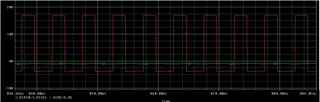
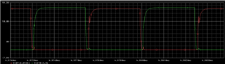
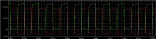
. when I replace the top mosfet with a capacitor (gate to source with same Ciss 2124p) this is working normal.

  • Hi Swathin,

    Thanks for following up with these details.

    That is interesting that it works with a MOSFET replaced by a capacitor.

    Can you share the schematic and waveform of this?

    Regards,

    Hiroki

  • Finally i did able to simulate with MOSFET as well, with both +ve and -ve biasing, but its working when i am not applying any voltage across the MOSFETS. these are the output waveforms with and without 250V across MOSFETs (Red-Vout1, Green- Vout2, Blue -VDDA).    
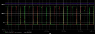
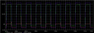
What is causing the VDDA to fall to zero volt when switching.

  • Hi Swathin,

    I see, thank you for sharing these images.

    I noticed in your schematic that VDDA and VDDB pins are shorted together which is likely disrupting the bootstrap circuit.

    Try changing the connection to be like this:

    Let me know if this helps!

    Regards,

    Hiroki

  • Hi Hiroki,

    Thanks that resolved my issue, am getting pulses at outputs but there is a slight curving at the rising edge of the pulse, compared to the falling. And  small spikes as well   
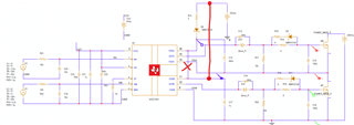
how to resolve this.

  • Hi Swathin,

    Glad that fixed the issue with the channel A output.

    The first approach I would try is to increase the bootstrap capacitor value. It may not be providing enough power during the Miller plateau region of the turn-on which may result in that slight dip.

    For the turn-off, try playing around with the turn-off gate resistor value to see if this has an effect on the small voltage spike after the turn-off.

    Hopefully this helps.

    Regards,

    Hiroki

  • Hi Hiroki, 

    we selected the " Negative Bias with Zener Diode on Iso-Bias Power Supply Output " configuration since the bootstrap method requiring higher peak input current from the source. i have some doubts in component selection for this configuration.

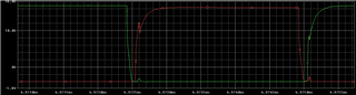
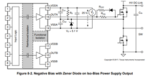
     How to select the capacitor values for CA1 and CA2? in this configuration

  • Hi Swathin,

    I would recommend a value between 220nF and 10uF for the CA1 and CA2 decoupling capacitors. An additional 100nF capacitor in parallel will also help with high frequency filtering.

    The Rz in this configuration of negative bias is there to set the Zener current which can be configured using the IV characteristics of the Zener diode.

    Regards,

    Hiroki

  • hi Hiroki, thanks for your response.

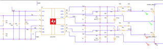
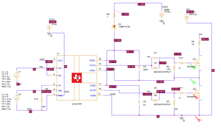
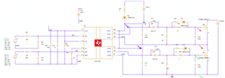
      this is the schematic i made for the application but

    1. if you check the output waveform upper side gate out is not going to negative side. if remove the ground connection from mosfet bridge the lower side wont go to negative. 

    2. if you check the schematic from datasheet there is one more capacitor parallel to the  supply how to calculate the value for that one.

  • Hello Swathin,

    Hiroki must be away from his office at this time. He should respond to your question within the next business day.

    Regards,

  • Hi Swathin,

    1. if you check the output waveform upper side gate out is not going to negative side. if remove the ground connection from mosfet bridge the lower side wont go to negative. 

    From the schematic, it looks like the probing point for the low-side output is being referenced to the 0 ground which would pull the signal to 0V.

    2. if you check the schematic from datasheet there is one more capacitor parallel to the  supply how to calculate the value for that one.

    This capacitor is the bulk decap that will provide instantaneous power to the gate driver. A 50V 10uF MLCC will be sufficient for this capacitor.

    Regards,

    Hiroki

  • Thanks Hiroki,

    That solved the issues 

  • Hi Hiroki,

    i have one more doubt. As per the Equations provided in the data sheet the total power Required for one side is  0.4472W  but in simulation the minimum i could achieve is 1W. Can you please check this and let me know where i did wrong?. the losses from zener and its limiting resister (2.4k) Iis not considered in equation i guess.

    1 Gate Driver Static power Loss (PGDQ)
    VVCCI 5 V
    IVCCI 0.0027 A
    Quiescent power loss on the driver 0.0135 W
    VVDDA 21 V
    IDDA 0.0025 A
    VVDDB 21 V
    IDDB 0.0025 A
    Driver self-power consumption 0.105 W
    Gate Driver Static power Loss (PGDQ) 0.1185 W
    2 Gate Driver Switching power requirement(PGSW)
    VDD 21 V
    QG 7.94E-08 C
    Fsw 200000 Hz
    PGSW 0.66696 W
    3.1 Gate driver loss on the output stage (PGDO)Linear Pull-Up/Down Resistor:
    ROH 5
    RNMOS 1.47
    RON 5
    R_GFET_Int 1.14
    ROL 0.55
    ROFF 1.42
    Linear Pull-Up Resistor 0.143146
    Linear Pull-Down Resistor 0.176849
    PGDO_HS 0.047736 W
    PGDO_LS+HS 0.106712 W
    Single Driver Driving Single MOS Total Power Requirement for the Gate Driver Supplies = PGDQ+PGSW+PGDO_HS 0.447216 W  
    Taking 50% Tolerance - Gate Driver Power Required for  A Side Gate Driver is   0.670825 W
    High Side Channel ()W Each  0.670825 W Each
    Low Side Channel - W  2.012474 W
    Total Power Requirement for the Primary side 4.024948 W
      Total power requirement for 1 Driver 0.670825 W        
    Single Driver driving Dual MOS Total Power Requirement for the Gate Driver Supplies = PGDQ+PGSW+PGDO_LS+HS 0.892172 W Without Bootstrap
    Taking 50% Tolerance - Gate Driver Power Required for Both A&B Side of Gate Driver is   1.338258 W
    High Side Channel ()W Each  0.669129 W Each      
    Low Side Channel - W  2.007387 W
    Total Power Requirement for the Primary side 4.014774 W
      Total power requirement for 1 Driver 1.338258 W        
  • Hi Swathin,

    From the values you have provided, the calculations look correct.

    Do you mind sharing more details about the simulation schematic? Just want to see all of the possible factors that could be included in the simulation that would not be included in the datasheet equations.

    Looking forward to hearing back.

    Regards,

    Hiroki

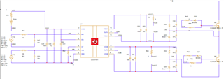
  •  power mos p parameters are edited as per real switch bias voltage is coming from ucc25800 based power supply

  • Hi Swathin,

    Thank you for the details.

    The power loss calculations in the datasheet will include the total power loss inside the gate driver as well as the switching losses.

    Bootstrap and negative bias circuitry will not be included in the datasheet calculations.

    Could you try measuring the losses from the negative bias network in your schematic to see if the additional power loss is coming from there?

    Regards,

    Hiroki

  • Zener diode have 33mW and Zener series resister have 164mW losses measured.

    FROM SIMULATION    
    Driver input current 0.041 A
    Driver input Voltage 24.040 V
    Driver input Power 0.986 W
    RZ Dissipation 0.164 W
    Zener dissipation A 0.033 W
    Ron dissipation B 0.144 W
    Roff dissipation C 0.065 W
    Diode dissipation D 0.013 W
    MOSFET dissipation (Source, drain disconnected ) F 0.094 W
    Total Surrounding component dissipation (A+B+C+D+F) 0.513 W
    IC dissipation (Total-Surr.) 0.473 W
    Switching Dissipation (total-IC) 0.513 W
  • Hi Swathin,

    Thanks for following up!

    Adding up the total gate driver power required for the driver supplies with the negative bias Zener circuit as well as any ESR from the capacitor models, the total power loss should be closer to your simulated values.

    Hope this helps with the question.

    Regards,

    Hiroki