This thread has been locked.

If you have a related question, please click the "Ask a related question" button in the top right corner. The newly created question will be automatically linked to this question.

TPS7A94: Layout and Schematic review

Part Number: TPS7A94


Tool/software:

Hi All,

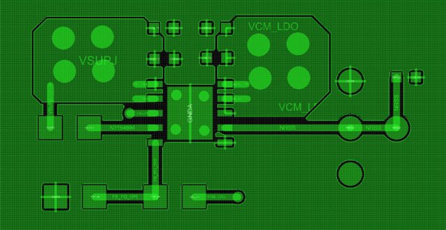
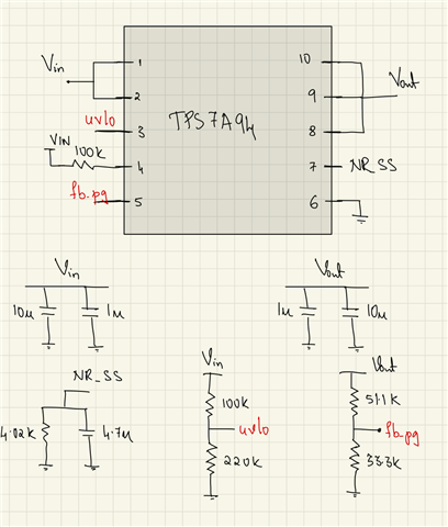
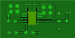
I needed a review for my schematic and layout (images attached). I want the output of the LDO to be 0.6V with a supply voltage of 5V. (As the output voltage is less than 1.2V, the current limit is set to 100% by default). Please let me know if anything needs to change. (I am using a potentiometer for NR/SS resistance control) I am new to PCB design and hence, any help would be greatly appreciated. 

Thanks in advance,

Nishanth

  • Hi Nishanth,

    My only comment for the schematic is that pulling PG up to VIN instead of VOUT will result in PG falsely being pulled high while VIN is ramping when instead it should be off. This is because the PG circuit needs enough voltage to exceed the VGS threshold of the open-drain transistor to be able to pull down PG when the output is not at regulation. For this reason it's better to pull PG up to VOUT.

    Now for the layout, my first question is what is the expected load current for your application? Since this device is capable of sourcing 1A, if you intend to use it at max load there will be (5V - 0.6V) * 1A = 4.4W, which is too much for almost any LDO. This is a potential issue in general, but the thermal issue is made worse by the way the thermal pad is laid out. The top-layer copper (or same side, whichever side the device is soldered on) is the most effective at removing heat, and the way you have drawn it, the thermal pad is only connected by thin copper traces. You should make the thermal pad connection to the top-layer copper continuous, like below. The thermal vias you have under the thermal pad are good, but you could improve the heatsinking by squeezing more vias in. It's recommended to use as many minimum-sized vias that you can fit under the thermal pad to maximize thermal performance. The minimum size is dependent on the PCB manufacturer and which PCB fabrication package you are looking at (smaller minimum size usually comes at a higher cost). With that said, if you are not using this device close to its rated maximum current then the thermal concern may not be as bad, but either way the thermal pad connection should be stronger. 

    You have placed the NR/SS cap and/or resistor pretty far away from the device. It would be better to put both the resistor and capacitor right across pins 6 and 7 since pin 6 is the device ground. There's no good reason to draw them away from the device so far, and doing so will add more parasitics.

    If you pull PG up to VOUT instead of VIN, you will have more room to put the EN_UV resistor divider right next to VIN and EN_UV. I can't tell exactly, but it looks like they might be on the other side of the board. 

    Regards,

    Nick

  • Hi Nick,

    I cant thank you enough for your valuable input. 

    1. I have pulled the PG upto Vin only using a 100k resistance. (As suggested by the datasheet, 4th pin is the PG pin)

    2. I agree, the thermal pad should be "strongly" shorted to the ground. The tool auto generated the small slither and I never bothered to change it. (It has happened with all my ICs in my PCB and I am changing it)

    3. I will make sure the resistance and the capacitance of the NR/SS are near the pins. 

    Again. I thank you for replying!

    Regards,

    Nishanth A B

  • Hi Nishanth,

    You're very welcome. 

    1. I have pulled the PG upto Vin only using a 100k resistance. (As suggested by the datasheet, 4th pin is the PG pin)

    What I said is true for most devices, but upon looking at this again, I misspoke. I believe PG is suggested to be pulled up to VIN for this device because of its low VOUT potential. If you pulled PG up to VOUT when VOUT = 0.6V, the PG signal will likely not correspond to a logic-high since 0.6V is pretty low, so pulling up to VIN does make more sense in this case. Sorry about that. 

    2. I agree, the thermal pad should be "strongly" shorted to the ground. The tool auto generated the small slither and I never bothered to change it. (It has happened with all my ICs in my PCB and I am changing it)

    Yes, you should be careful of using auto-routing tools, and only use it to route "unimportant" traces. I personally do all of the routing manually so that I can make informed decisions for each one. 

    Cheers!

    -Nick