


Tool/software:
Hello mike,
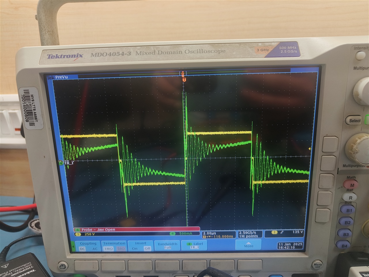
I have oscillations in transformer primary current waveform. Not seen in my earlier designs. Transformer primary voltage looks Ok.
Below is the waveform.
Output there is no RCD Clamp or RC snubber as of now.
Original question:

Tool/software:
Hello mike,
I have oscillations in transformer primary current waveform. Not seen in my earlier designs. Transformer primary voltage looks Ok.
Below is the waveform.
Output there is no RCD Clamp or RC snubber as of now.
