This thread has been locked.

If you have a related question, please click the "Ask a related question" button in the top right corner. The newly created question will be automatically linked to this question.

UCC27324-Q1: output resistance

Genius 4840 points
Part Number: UCC27324-Q1

Tool/software:

Our customer would like to ask about Revision History. Current datasheet have description following.

 Changes from Revision C (June 2018) to Revision D (November 2023) Page

 • Changed input threshold voltage values in Input (INA, INB) Electrical Characteristics......................................5

 • Deleted VOH output high level and VOL output low level, changed output resistance high and output resistance low values and deleted Latch-up protection in Output (OUTA, OUTB) Electrical Characteristics......................5

 • Changed title on Figure 5-2 and changed Figure 5-5 and Figure 5-6 ...............................................................6

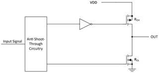
About " changed output resistance high and output resistance low values"

The value of output resistance of new IC appears to be decreasing on datasheet.

But measurement condition/method is different between new IC and old IC.  

Please let us know the detail of this difference. It would be helpful if you could explain with a diagram.

SLUS678D

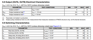
(2) Output pullup resistance here is a DC measurement that measures resistance of PMOS structure only, not N-channel structure

SLUS678B

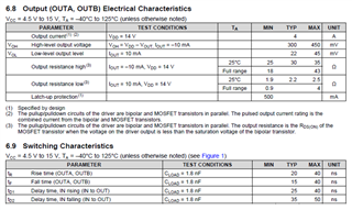
(3)The pullup/pulldown circuits of the driver are bipolar and MOSFET transistors in parallel. The output resistance is the RDS(ON) of the MOSFET transistor when the voltage on the driver output is less than the saturation voltage of the bipolar transistor.

Regards,

Kura

  • Hey Kura,

    Thank you for reaching out with the customers questions regarding the UCC27324-Q1.

    With the latest datasheet revision (D), there was an error that should have updated the block diagram of the output stages to the following:

    We are working to update this with the correct diagram.

    So, the resistance values from the datasheet refers to the FETs themselves here for the output stage pullup/pulldown circuits.

    This updated output structure with lower Rds(on) allows for better performance and so that is why we have made this change.

    Let me know if there are further questions.

    Thank you,

    William Moore

  • William-san

    Thank you for your support.

    Our customer has additional questions.

    (1) When will the block diagrams  of the output stages in the datasheets be changed?

    (2)Why do the SW characteristics not change even though the output stage configuration has changed?
        Please tell me the reason.

    (3In SLUS678B datasheet, There is description following

      The pullup/pulldown circuits of the driver are bipolar and MOSFET transistors in parallel. The output resistance RDS(ON) of the MOSFET 

      transistor when the voltage on the driver output is less than the saturation voltage of the bipolar transistor.

      -> What is the saturation voltage of a bipolar transistor?

    Regards,

    Kura

  • Hi Kura San,

    Due to the holiday in the US on 20th Jan 2024, many of the device experts are currently out of the office. When they return, they will look into this and provide a response. Please expect some delay accordingly.

    Thanks,
    Pratik

  • Hey Kura,

    Thank you for your patience.

    1. These will be included in our next revision. I do not have a timeline for that at this time.

    2. The new output stage was designed to target and maintain the same switching characteristics to minimize impact to customer systems.

    3. As shown by the output stage diagram that I shared above, there is no longer a bipolar portion of the output stage, there is just the pullup/pulldown FETs.

    Thank you,

    William Moore