


Other Parts Discussed in Thread: TPS40060EVM, LM5146, TPS40060
Tool/software:
Hello people,
We have a design with a TPS40061, which can modulate the voltage with a switched resistor at the feedback. We are now changing it in a way that will result in more current beeing fed back, when reducing the set voltage and are now facing big problems with the design.
First we thought it was dynamic behaviour due to the set voltage step and the compensator not beeing designed right but with a well enough designed compensator we managed to make the problem show up in steady state condition, without switching anything, so a compensator reaction is out of the question. We boiled the setup down to a modified TPS40060EVM with a TPS40061 installed with, the same values for output capacitance and inductor used in our design and a current source at the output, that feeds current back to the input. A large resistor takes that current because our voltage source is not bidirectional.
Here is the schematic. I have also marked the colors for the signals in the next plots:
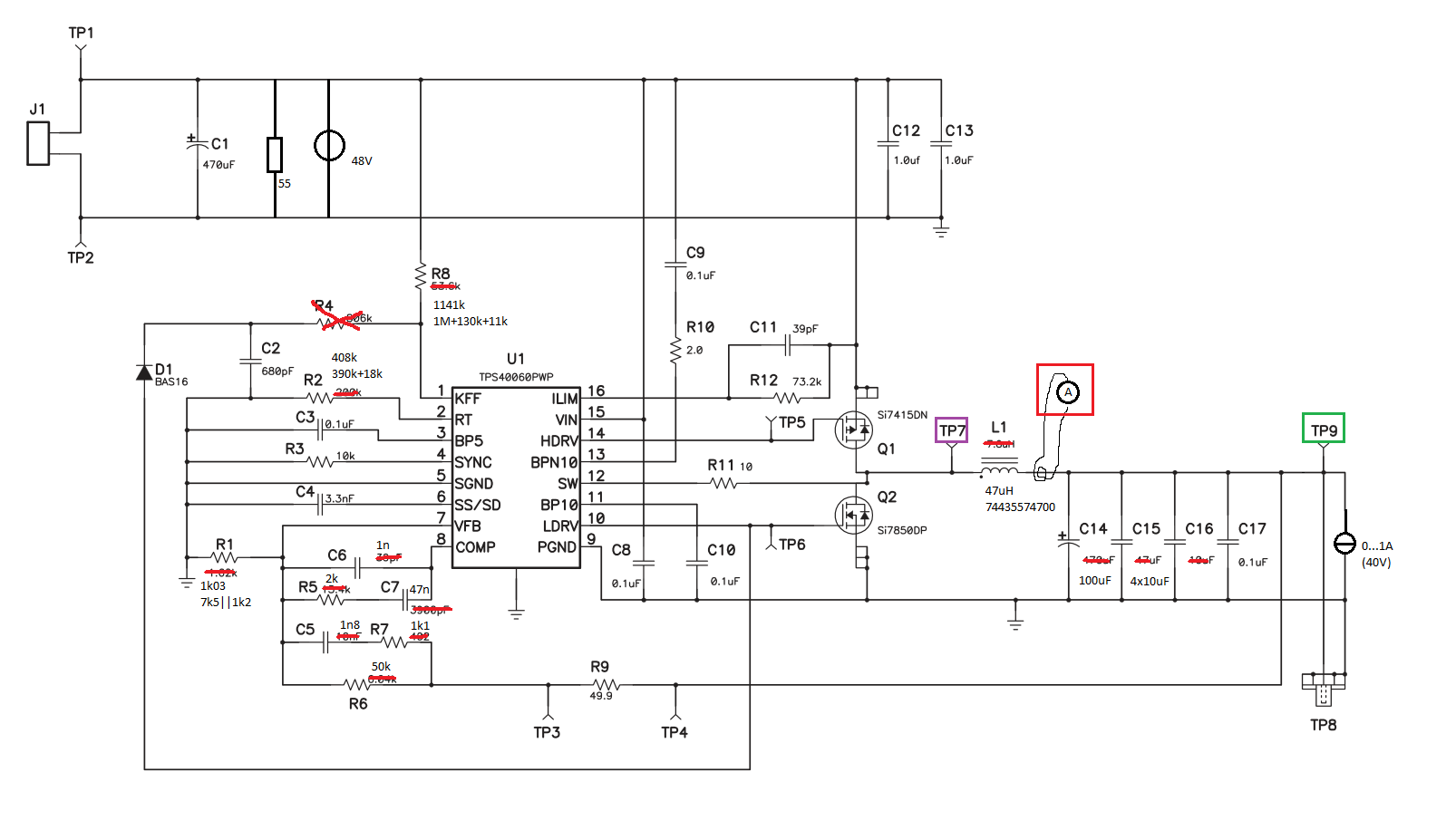
The problem is both mosfets sometime switching off at certain voltage ranges, beginning at certain reverse currents. I assume that the bottom mosfet was supposed to turn on, but the gate does not get any voltage in these cases. The top Mosfet sometimes shows the current flowing through the body diode and it also sometimes clamps an oszillating voltage, which I assume to be ringing between the inductance and the FETs. The result sometimes also makes the regulation oscillate and very susceptible to dynamic changes (changing the current or the input voltage) and sometimes even shuts off completely. We suspect an undocumented protection feature, especially when the controller shuts off completely at high reverse current and voltage jumps.
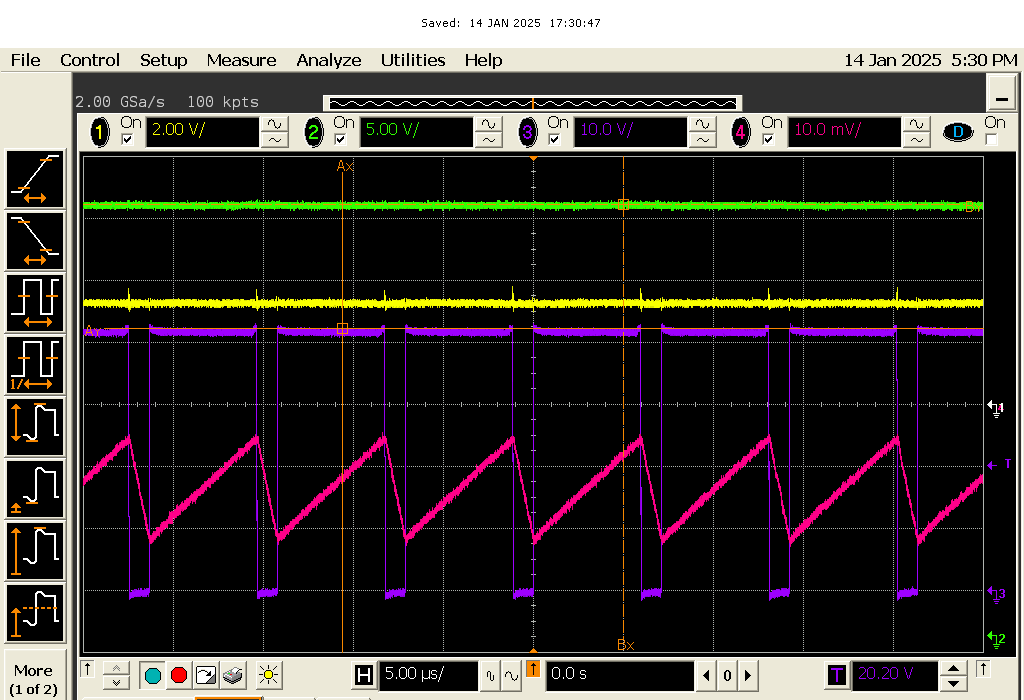
This is normal behavior at 42V at a current that always results in negative current through the inductor. Yellow is not interesting, I forgot to turn that channel off. Green is the output voltage, which is also not very important. Blue is the switching node voltage and red is the inductor current at 500mA/Div.
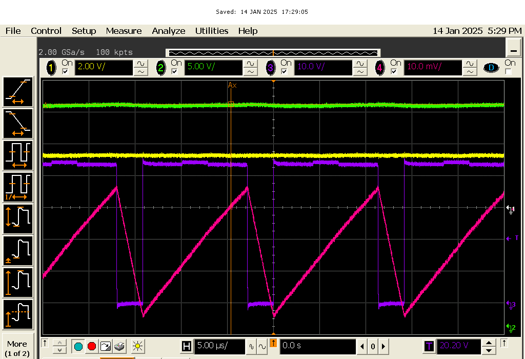
At 42.5V and 700mA of current this pattern emerges with every second low side swichting cycle replaced by the positive mosfet clamping the voltage. This results in half the switching frequency.
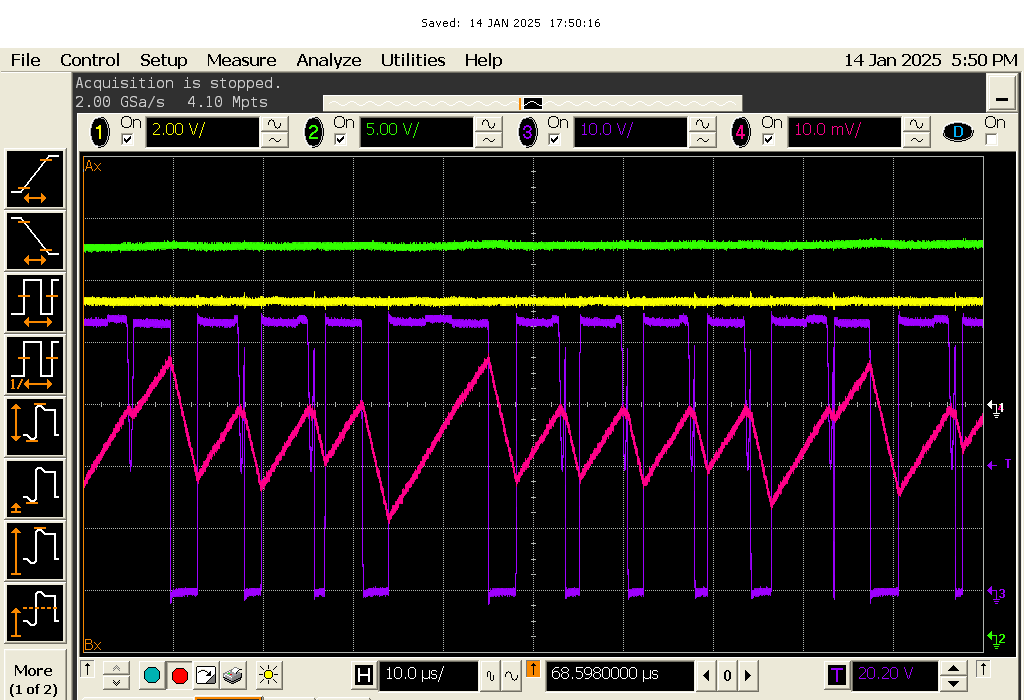
At 500mA, same voltage, after the Pmos clamps the voltage for some time, ringing occurs and the bottom mosfet even turns on sometimes.
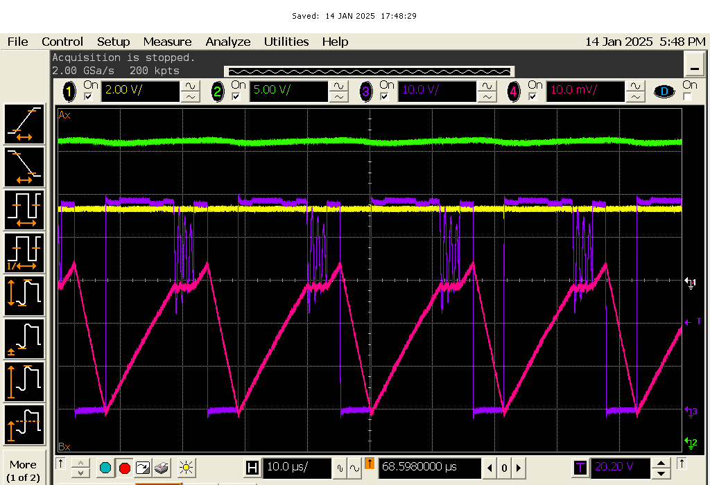
Increasing the voltage or the current can result in more chaos, like this.
If the input voltage is at 48V or beyond and a current above 200mA is switched on, it will shutdown entirely. It will also react that way, if the input voltage is at the lowest possible (About 40V)a current of 1A (It is working fine in this condition) is added and the input voltage slowly turned up up to about 45V. Lower current has a lower voltage threshold. The regulator might recover, if the input voltage is reduced again, though there is a noticable hysteresis.
So what could the problem be? Is it some undocumented protection feature? Some parasitic effects, that could be filtered away? I can not even think of a good reason for both mosfets being turned off, as only undervoltage lockout and overcurrent protection could be able to do that. It could not be overcurrent protection, as it is only active while the top mosfet is turned on. All other voltages seem fine.
I would be very thankful for any pointers and will gladly take additional measurements and update here, if you need any.
