Tool/software:
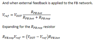
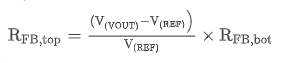
I've tested configuring VOUT with internal feedback on this chip and it works flawlessly. In the process I did my own code to set this up dynamically through I2C, for which the formulas provided in the datasheet were of great help. I currently do not have the hardware to test this for the external feedback scenario, and I'm having a hard time making sense off of your formula for the FB external division rate, retrieved from the following formula: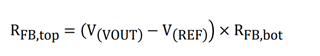
Doing the math myself I've been unable to reach this value at all. In the process I assume the control amplifier for the output voltage loop regulates the system to achieve the VOUT_A DAC voltage at all times in the node between RFB top and bottom resistors. From there I calculated a simple voltage divider but I do not get where the formula is coming from. Let me know where I'm mistaken here