Other Parts Discussed in Thread: TPD2S300, , BQ25713, BQ25792, BQ25756, BQ25731
Tool/software:
Dear Expert:
I have a few questions about the application of TPS25751D+TPD2S300YFFR. Our application scenario is that the Bluetooth speaker requires input 9V3A/5V3A, and the output requires 5V3A. Help to answer it, thank you. Which feet are used to burn the program, and whether the Bluetooth end can upgrade the chip TPS25751D online through I2C.
2. According to the schematic diagram of the EVM board, there is an external EEPROM. Is this EEPROM necessary? What are the specifications and the minimum Kb required?
3. If the TYPE-C terminal does not support BC1.2, does the DP/DN network need not connect to GPIO4/GPIO5 of the TPS25751D?

4.TPS25751 with TPD2S300 circuit, with 4 MOS tube, are there any specifications for MOS tube, such as current (D-S), or Ciss requirements?

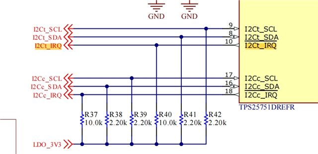
5.VIN 3V3 pin, external LDO power supply, this need to be always powered? Do you need to supply power when the USB is not inserted in battery mode? If the battery is out of power, where does this voltage come from? 6. The two groups of I2C on the EVM board are connected to the main control chip. Do we need two groups of I2C to connect to the main Bluetooth chip in our design? What are the two groups of I2C used for respectively?
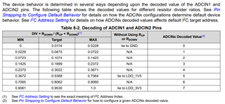
7. For the battery is double battery 8.4V, the input needs to support 9V/3A,5V/3A, the external output supports 5V3A requirements, how to connect the ADCIN1,ADCIN2 circuit

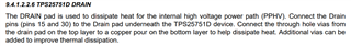
8. The 15th, 30th and 40th feet of TPS25751D need to be suspended. I think the EVM board is suspended.

10. Can the GPIO port of TPS25751D be used as an ordinary IO port to configure input and output?

11. How is TPS25751D reset?
12. GPIO NF and GPIO PF on the EVM board must the two networks be pulled up R63 and R64(connected to 3.83K)
13. Since the voltage rise and fall path of the charging chip is the same power network (9V3A/5V/3A input, 5V/3A output), should PP5V and PPHV be short-circuited together? Or is the PP5V suspended and only connected to the PPHV?