


Tool/software:
I've built a prototype board which has TPS552872RYQR set up for 3V output voltage. Functionally the design works as intended in my application, but I noticed a curious mismatch of observed leakage current into VOUT compared to the datasheet specification.
Datasheet lists VOUT leakage current of 1uA typical, 20uA max when device is disabled. I am however measuring significantly more than that- approx 160uA.
Schematic of this part:
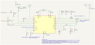
I'm applying 8V on VCC and have removed FB2 for testing to make sure the leakage comes from U1 instead of the rest of the circuit.
With BUCKBOOST_EN floating or logic 0, voltage on VOUT is measured at 4V. When I add 1k resistor to ground (after the feedback path), the output voltage drops to ~160mV.
I've also tried operating the IC without +3V3 rail present (to exclude the potential leakage paths via internal protection diodes on logic pins), which did not change the observed leakage.
The question I have is- are there any other leakage paths to VOUT that I'm missing? Is the observed behaviour expected?
