This thread has been locked.

If you have a related question, please click the "Ask a related question" button in the top right corner. The newly created question will be automatically linked to this question.

LM5176: Wind Turbine Schematic and Application Review

Part Number: LM5176

Tool/software:

Hello,

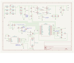
I made a new USB-C charging circuit schematic, which involves an LM5176 as the regulator. The input comes directly from a 3 phase wind turbine, then gets rectified via diode bridge.

Here are the design parameters which I need:

VIN minimum: 2.5V

VIN maximum: 24V

Programmed VOUT Voltage: 5.2V

IOUT Expected Operating Amperage (Per USB-C spec): 1.6A

I built the schematic based off of the recommended schematic provided by the TI WEBENCH Power Designer Tool. However, after designing the circuit, I learned that there is also a calculator tool specifically made for the LM5176.

The Calculator tool doesn't seem to match what the WEBENCH tool provides, and I would like some input from someone else to help me decide what parameters are optimal.

For instance, since this is intended to be powered from a wind turbine, the input voltages will vary by a large amount. The turbine typically outputs anywhere from 0V with no wind, to 20V on the windiest of days. On average, it runs between 3V and 10V. Due to the large variance of input voltages, I'm having a hard time determining an optimal frequency setting.

One other thing to note, the calculator tool is telling me that the output capacitor ESR should be less than 44.8milliohms, but the aluminum output capacitors which WEBENCH recommended all have higher ESR than that.

Finally, I also would like some advise on the compensation design, such as optimal crossover frequency, resistor values, and capacitor values. Once again, WEBENCH suggests values that are different from the calculator tool. I also noticed that the datasheet illustrates Cc1 to be on top of Rc1, but shows the opposite on the schematic in the calculator tool.

In conclusion, here are the parameters I'm not so sure about:

1: Switching Frequency

2: Output Capacitor ESR

3: Compensation Design Component Values (Rc, Cc1, Cc2)

4: Rs value

Below is a copy of the schematic, which was originally designed from the WEBENCH recommendations, with corrections in blue text based off of what the calculator tool showed me.

Below is a copy of the calculator tool with some parameters that I input:

Copy of LM5176 Buck-Boost Quickstart Tool.pdf

  • Hi Stephen,

    The Webench Tools is a very generic tool which provides a solution including components for the power stage. Therefore the restrictions here are much higher.

    The Quckstart tool allows you to due more optimizations and go deeper into the design therefore there are difference here.

    To your questions:

    1. selecting the right switching frequency is as for most of the parameter finding the right balance for your application between size, efficiency and cost.

    For the switching frequency this does apply as well, e.g. lower switching frequency often gives higher efficiency but requires a larger inductor.

    2. the ESR of the output cap impacts the the ripple voltage on the output. Therefore this needs to be selected to fit for your output ripple requirement.

    3. Compensation needs to be set based on the whole loop. Here the switching frequency, inductor, output cap and ESR,.... will have the major impact.

    For selection the Quickstart calculator can help but the following rules should be applied:

    Cross over frequency the lower of 1/10 f_SW or 1/5 or RHPZ

    Phase margin > 60 Degree

    Gain margin > 12 dB

    See also

    Switch-Mode Power Converter Compensation Made Easy | Video | TI.com

    Download white paper: Switch-Mode Power Converter Compensation Made Easy

    4. Rs set the peak inductor current limit and helps to protect your power stage. This needs to be set low enough to enable the power stage to properly provide the required output current and high enough to ensure the components you have selected can not get damage due to overload in case of e.g. short at the output.

    For deeper dive into the design of a power stage the video series is great:

    Experimental power electronics curriculum and reference | TI.com

    Best regards,

     Stefan