Tool/software:
The BQ25887 does not initiate charging when a USB power source is connected. Charging begins only after plugging and unplugging the USB power source three times.
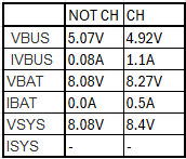
- Power Good Indicator: Initially lights up but turns off shortly thereafter.
- VBUS Measurement: VBUS voltage remains at 4.6V–4.7V even when the Power Good indicator turns off.
- Register Configuration: Default settings (no modifications have been made).
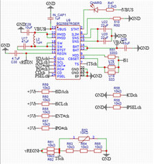
- External Components: PSEL and CD pins are pulled down with 10kΩ resistors.
- Hardware config: same as the example in the datasheet.
thanks for the help solving this 
Registers while not charging:
- Cell Voltage Limit............... (0x0): 0b10100000
- Charge Current Limit............... (0x1): 0b11011110
- Input Voltage Limit............... (0x2): 0b10000100
- Input Current Limit............... (0x3): 0b111001
- Precharge and Termination Control (0x4): 0b100010
- Charger Control 1.................. (0x5): 0b10011101
- Charger Control 2.................. (0x6): 0b1111101
- Charger Control 3.................. (0x7): 0b10
- Charger Control 4.................. (0x8): 0b1101
- ICO Current Limit.................. (0xA): 0b0
- Charger Status 1.................. (0xB): 0b1000
- Charger Status 2.................. (0xC): 0b110000
- NTC Status........................ (0xD): 0b0
- FAULT Status..................... (0xE): 0b0
- Charger Flag 1..................... (0xF): 0b0
- Charger Flag 2..................... (0x10): 0b0
- Fault Flag........................ (0x11): 0b0
- Charger Mask 1..................... (0x12): 0b1110000
- Charger Mask 2..................... (0x13): 0b0
- Fault Mask........................ (0x14): 0b0
- ADC Control........................ (0x15): 0b110000
- ADC Function Disable............... (0x16): 0b0
- IBUS ADC1........................ (0x17): 0b0
- IBUS ADC0........................ (0x18): 0b0
- ICHG ADC1........................ (0x19): 0b0
- ICHG ADC0........................ (0x1A): 0b0
- VBUS ADC1........................ (0x1B): 0b0
- VBUS ADC0........................ (0x1C): 0b0
- VBAT ADC1........................ (0x1D): 0b0
- VBAT ADC0........................ (0x1E): 0b0
- VCELLTOP ADC1..................... (0x1F): 0b0
- VCELLTOP ADC0..................... (0x20): 0b0
- TS ADC1........................... (0x21): 0b0
- TS ADC0........................... (0x22): 0b0
- TDIE ADC1........................ (0x23): 0b0
- TDIE ADC0........................ (0x24): 0b0
- Part Information.................. (0x25): 0b101001
- Cell Balancing Control 1......... (0x28): 0b101010
- Cell Balancing Control 2......... (0x29): 0b11110100
- Cell Balancing Status and Control (0x2A): 0b11000000
- Cell Balancing Flag............... (0x2B): 0b0
- Cell Balancing Mask............... (0x2C): 0b0
registers while charging:
- Cell Voltage Limit............... (0x0): 0b10100000
- Charge Current Limit............... (0x1): 0b1011110
- Input Voltage Limit............... (0x2): 0b10000100
- Input Current Limit............... (0x3): 0b111001
- Precharge and Termination Control (0x4): 0b100010
- Charger Control 1.................. (0x5): 0b10011101
- Charger Control 2.................. (0x6): 0b1111101
- Charger Control 3.................. (0x7): 0b10
- Charger Control 4.................. (0x8): 0b1101
- ICO Current Limit.................. (0xA): 0b10
- Charger Status 1.................. (0xB): 0b1100
- Charger Status 2.................. (0xC): 0b10110010
- NTC Status........................ (0xD): 0b0
- FAULT Status..................... (0xE): 0b0
- Charger Flag 1..................... (0xF): 0b1000001
- Charger Flag 2..................... (0x10): 0b10010010
- Fault Flag........................ (0x11): 0b00001000
- Charger Mask 1..................... (0x12): 0b1110000
- Charger Mask 2..................... (0x13): 0b0
- Fault Mask........................ (0x14): 0b0
- ADC Control........................ (0x15): 0b110000
- ADC Function Disable............... (0x16): 0b0
- IBUS ADC1........................ (0x17): 0b0
- IBUS ADC0........................ (0x18): 0b0
- ICHG ADC1........................ (0x19): 0b0
- ICHG ADC0........................ (0x1A): 0b0
- VBUS ADC1........................ (0x1B): 0b0
- VBUS ADC0........................ (0x1C): 0b0
- VBAT ADC1........................ (0x1D): 0b0
- VBAT ADC0........................ (0x1E): 0b0
- VCELLTOP ADC1..................... (0x1F): 0b0
- VCELLTOP ADC0..................... (0x20): 0b0
- TS ADC1........................... (0x21): 0b0
- TS ADC0........................... (0x22): 0b0
- TDIE ADC1........................ (0x23): 0b0
- TDIE ADC0........................ (0x24): 0b0
- Part Information.................. (0x25): 0b101001
- Cell Balancing Control 1......... (0x28): 0b101010
- Cell Balancing Control 2......... (0x29): 0b11110100
- Cell Balancing Status and Control (0x2A): 0b11010000
- Cell Balancing Flag............... (0x2B): 0b10000
- Cell Balancing Mask............... (0x2C): 0b0