This thread has been locked.

If you have a related question, please click the "Ask a related question" button in the top right corner. The newly created question will be automatically linked to this question.

UCC28600

Other Parts Discussed in Thread: UCC28600, TL431, TINA-TI, TLV431A

Hello,


I am copying a ti circuit using 28600 for a 400v-12v converter, the TI's example part number is PR798.5824.PR798B-2_SCH NC.pdf

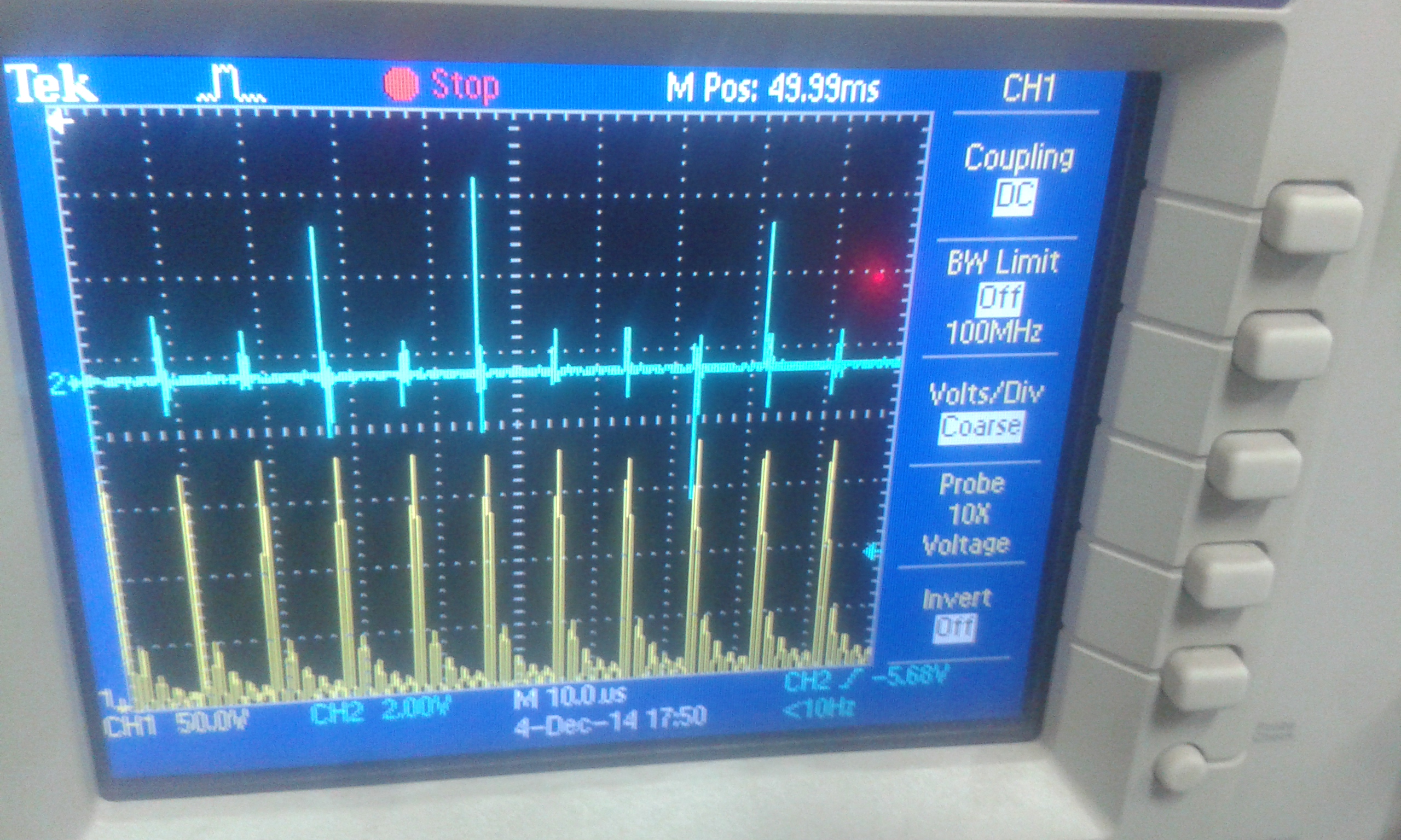
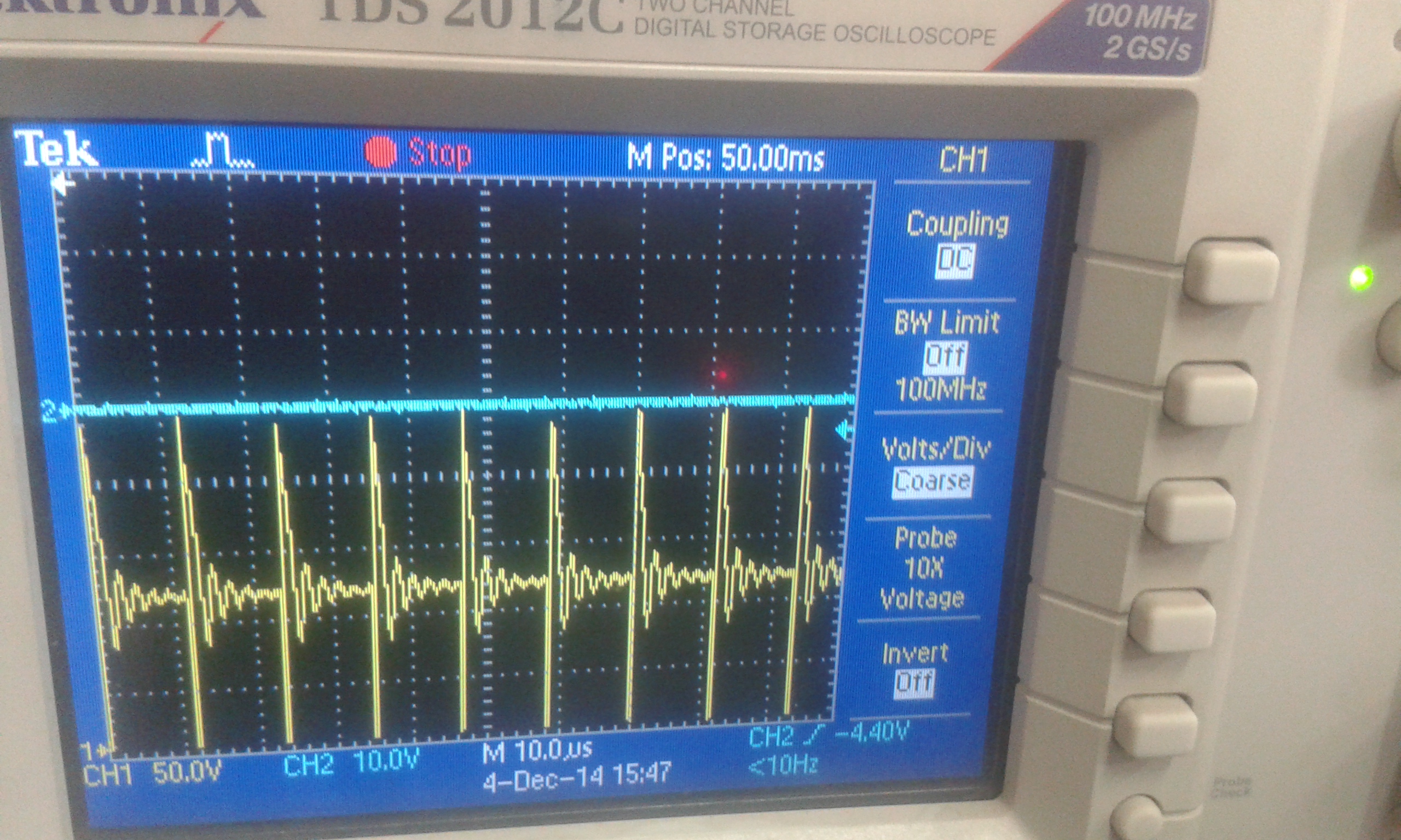
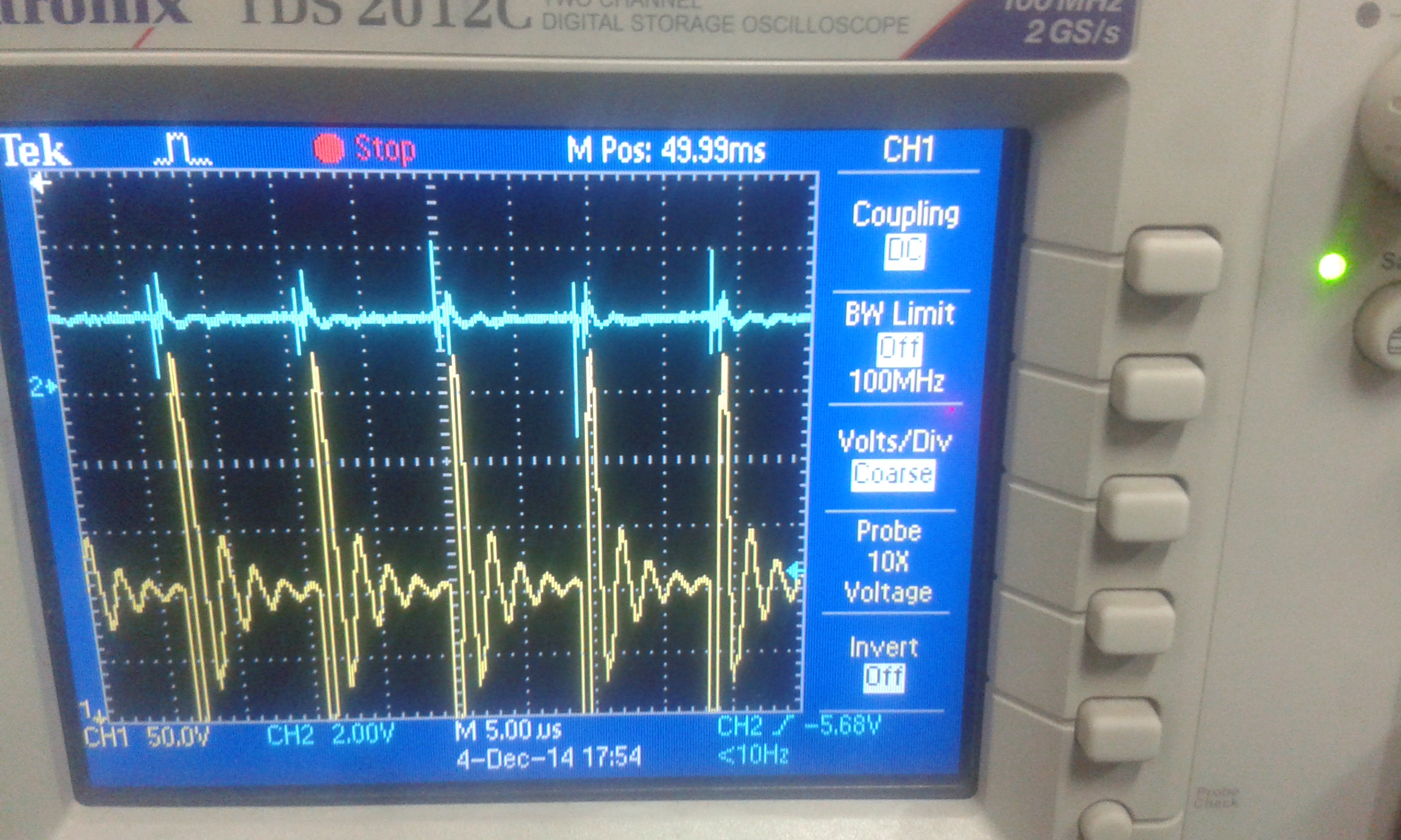
but my board is on an off all the time, from the oscilliscope , the power supply pin of the chip fluctrates ,lower than shut down threshold; then it shut sdown for a while.later it turns on again.

however, as the chip relys on the bias winding of the transformer, if the circuit is not working , then the winding cannot provide the nesssery bias for itself.

so this is a bit hard to identify the problem.

any one has some clues/tips?

how the output capacitance of mosfet could affect the circuit? we only changed the mosfet of which output capacitance is 12pf compared with the original 50pf.

thanks


  • ok, thanks guys, I found the problem.

  • i am glad you resolved the issue.  So, what was the problem?  Many other users may have this same issue and you could be of great assistance by sharing your experiences.

  • Also, please be sure to update the Design Calculator with the actual output capacitance of the MOSFET used.  The Coss of the FET is required to calculate the resonant time and the required magnetizing inductance for proper operation over the entire operating range.  It is important to fill in the design calculator inputs with as much information as possible for a robust and reliable design in the shortest amount of time.

  • I also have a similar problem with my 120V to 5V converter.  I am using the UCC28600 and I see the VCC pin oscillate in voltage as it approaches the 13V turn on threshold.  What was you solution?  Thanks!

  • Check the SS pin.  For start up, the SS voltage must rise above FB (FB immediately rises to 5V at start up) to indicate "SS Done".  If it's getting discharged then the device is detecting a fault such as line overvoltage, output overvoltage, over current, REF_Okay not okay, or over temperature.  Assuminig the switch is not on long enough to generate an output over voltage, and he device has not hit thermal limit, the most likely suspects are the CS, line voltage, or Reference. 

    One thing that must be corrected on the schematic that you sent is there is no decoupling capacitor on VDD.  VDD must have a 0.1uF ceramic capacitor, placed with short traces between GND and VDD, this provides essential filtering for the internal REF-Okay signal. 

    FB is senstive to noise and using a 330pF to 390pF capacitor on it (instead of the 100pF that you have) may prove helpful.  Do not use more than 390pF on FB though as the timing with the internal 20k pull up may compromise operation. 

    Check the resistor values that you have on OVP.  If OVPThe values are despendent upon the minimum valley vlotage  on the bulk voltage input.  The bulk input voltage is dependent upon the bulk capacitor value.  If you are using half of the input capacitance as the referenced design, your bulk voltage is sagging considerably more and modifications to the OVP components, power limit resistor, current sense resistor, and may be even the primary inductance, may need to be made.


  • Hi Allen,

    Please check your feedback circuit, ususlly something in the feedback ciruit is wrong, then it causes oscillation.

    in my case, it is simple, the TL431 got blown somehow in a wierd way, once replaced it, I never have had any problems in many PCBs.

     Hope it helps,


  • Thanks to both of you (Lisa and Harrison) for your helpful comments; I will try some of the solutions that Lisa suggested.  I will also look more closely at the feedback and SS pins.

    Here is a more complete description of what I am currently seeing:

    Upon application of AC power, I see the VDD voltage, on pin 6 of the UCC28600 device, slowly rise to about 13 VDC and then start to oscillate between 9 Volts and 13 Volts. I don’t get any output signal to the MOSFET switch and therefor, there is no bias voltage generated by the transformer to maintain the VDD voltage. Simulations of my circuit, using the Tina-Ti spice simulator, don’t show this anomaly.  I have a 22uF ceramic capacitor placed very closely to the VDD pin (actually measures 22uF in circuit); however, the oscillating voltage that I see on the VDD pin has the predicted slow rise time, from the 2M series resistance, and then I see a very quick drop from 13V to 9V - this repeats forever.  I did try using a 75 volt DC supply and I lowered the 2M VDD series resistor low enough to allow the device to turn on.  This did allow the power supply to start to function - maybe this points to my need for larger filter capacitors afte the bridge rectifier.  The quick drop in VDD voltage still is confusing; I wouldn't have expected this.

    I will hopefully find a solution to this in the next few days and post my results to the forum.  Thanks again for your comments. :)

    Allen

  • Oh, and BTW, I am using the TI design example PMP5192 as a base design and I reduced the filter capacitor values from 4.7uF to 2.2uF to save room on the PCB.

    Allen

  • Reducing the input capacitors will require modifications to the OVP, CS, and PL resistor values as these values are depenent upon the minimum bulk valley voltage. 

  • Thanks for updating us with your results! 

  • Allen, try reducing that filter capacitor on CS.  I honestly believe that it should be 100pF, not 1000pF...that's way too much filtering.  Also,does the unit start up under no-load conditions? 

  • Hello Lisa,

    Thanks for your suggestions!  I will try reducing the capacitor on the CS pin to 100pF and see if that makes a difference.  The UCC28600 device doesn't start under any kind of load; I tried using no-load and using a 15 Ohm load.  I rechecked the PCB layout several times and it is okay; also, the component values all measure correctly.  I did try reducing the 2M series resistor on the Vdd pin to 100K Ohms, this time using a 75V DC supply and 120 VAC separately as inputs, and the device looked like it was working, but only when there was no load; the SS pin was still low in this state.  I guess this indicates some sort of error condition.   I will do some more measurements; I hope this all doesn't sound too scatter-brained at this point! :)  I'm sure I will find the answer with your assistance. - Allen

  • Okay it is now working!!  Thanks for your assistance Lisa.  I made the following changes:

    1.  The capacitor on the CS pin was changed from 1000pF to 100pF

    2.  I added a 0.1uF ceramic capacitor directly on the power pins of the UCC28600

    3.  I changed the capacitor on the FB pin from 100pF to 390pF.

    4.  I added a 22uF aluminum electrolytic capacitor across the 22uF ceramic capacitor feeding the VCC pin of the UCC28600.

    5.  My big mistake here, I changed the zener shunt regulator from my incorrect TL431A to the correct TLV431A; different VREF threshold between these devices.

    The real difference that made the device work was adding the 22uF Electrolytic capacitor across the ceramic capacitor.  This must have changed the ESR of the capacitor combination enough to eliminate some ringing that was affecting the UCC28600.  I will now experiment with capacitor values to get a correct value for my circuit layout.

    The device works well at no load and with a 350mA load.

    Thanks to all for your help.

    Allen

  • Glad to hear that the problem was resolved.

    I am just curious as I think the real difference should be the incorrect  TL431, adding 22uF aluminium cap at the input should not make the difference as the ESR of the ceremic is already low enough and the 22uF capacitance should be enough for this power rating as well.

    After you fixed the TL431 issue, did you try to remove the 22uF aluminum cap?

    just feel strange , but you know better for sure...


    have a great day.


  • Yes, I agree that is it a strange problem.  I did try the circuit again after fixing the TL431 issue and it still didn't work.  The UCC28600 was indicating that it was seeing an error condition of some kind by sending the SS line low when the SS voltage reached about 1 V; the device would not start and would just oscillate in this startup mode.  I think the problem was that the ceramic capacitor had too low of an ESR for my particular layout.  I have seen ringing occur in my other power supply designs when I use a capacitor with too low of an ESR (such as a ceramic capacitor); the inductance of the circuit traces combine with the low capacitor ESR to create an overvoltage condition due to ringing of the quick voltage transients.  I have been able to solve this by adding a higher ESR capacitor in parallel with the ceramic to provide the current surge ability with ringing suppression from the higher ESR capacitor.  I hope this explains my intentions.  I am thinking that the ringing on the VDD line was causing some internal problems that shut down the device; but this is just a guess.

    Well, you know, anything is possible.  I was moving fairly quickly through my tests yesterday.  Maybe I should try the 22uF ceramic again in case I missed something and the circuit was really working with just the TL431 change, but I don't think so.

    - Allen

  • Is there an alternate source for the transformer used in the PMP5192 Rev. B design (AC input, 5 VDC output)?  The transformer is a GCI part number: G094279LF.  This device has a large lead time and I was wondering if there are alternate devices that were considered in a similar sized package.

    Thanks - Allen

  • The transformer was a custom design for that application so the chances of finding an off-the-shelf version are pretty slim.  We try to use standard core sizes, standard core materials, and standard bobbins so the lead time is minimized but not quite as short as standard catalog parts.  Unfortunately, because these devices are custom, it's difficult to second source them as the actual design belongs to GCi. 

  • Okay, thanks Lisa! :)

  • Just let you know, Ti has a good 12v-5v dc/dc part which is very small and meets many requiremnets in some embedded applications.

    you can try to just add this one to get your 5v from 12v, you won't lose too much efficiency as the original 12v flyback needs minmum load current to run anyway.

    For your information.

  • I'm curious as to why you think the UCC28600 needs a minimum load?  The device is designed for minimum power consumption at no-load for green initiatives.  The converter should regulate in a hysteretic burst mode for no-load and light load operation. 

  • Hi Lisa,


    Your curiosity makes sense as I didn't describe it correctly.

    In my application, UCC28600 circuit not only serves a 12v dc/dc but one auxillary winding of the transformer gives feed back on input voltage, say , 400v .

    When UCC28600 works in green mode, the feedback input voltage is much lower since the chip works in intermittent mode as you know.

    if the input voltage is not good, my downstream converter would not work.

    Thus, I have to add a minimum load to force the chip to get out of the green mode in order to get continuous oscillation to make the filtered signals to the right level.

    I hope this time I described it correctly.

    Thanks, 


  • I see, thanks for the clarification.  Yes, the other slave outputs will lose regulation due to the extended time between burst cycles.  Have you tried to minimize your "dummy" load by superimposing a small offset into CS so that the UCC28600 will transition out of burst at lighter load?

  • Hi Lisa, thanks for this smart idea.

    this means creating a negative offset on CS , right?

    it is not easy, do you have solutions?

    Thanks,

  • Actually what you want to do is to add a positive offset to CS but only during burst mode, or lightload hysteretic operation.  This would be the same procedure as reducing audible noise that  is explained in the Design Considerations app note (SLUA399) section 4.  The idea is that the STATUS signal is used to forward bias a diode that allows a small (100mV or so? I forget...) offset to be added to CS so that the converter thinks the current is high enough  to kick it out of hysteretic mode and into FFM.  You only want this offset superimposed on CS during burst mode because in all of the other modes there's an internal power limit offset already added to CS and if both offsets are there the controller will hit power limit.  Luckily, STATUS is high during burst and low in the other modes...

  • Allen:

    Could you upload you updated shematic to guys, let us to share it ,thanks!

  • adding an offset to CS during burst mode is shown in Figure 5 and explained in section 4 of http://www.ti.com/general/docs/lit/getliterature.tsp?literatureNumber=slua399b&fileType=pdf

  •  

    Hi Lisa,

    Where could I find the gerber files for this module discussed here?

    PR798.5824.PR798B-2_SCH NC.pdf

    I only find the schematic.

    Thank you,


  • Hi Lisa,


    Thanks a lot.


  • hello,

    i am ucc28600 to deliver 5V@10A output,

    the device shutsdown when i increase the load upto 2A,my question is how can i increase the load upto 10A, in calculated values using QR design tool,

    here are waveforms captured at Vin = 110VDC & Vout  = 5V at 800mA load

    i) cs pin voltage- channel 1,RCS = 375mE,RPL =1.2K

      mosfet drain voltage - channel 2

    ii) OVP pin vltage , Rovp1 = 288K,Rovp2 = 44.2K

    iii) mosfet drain voltage

  • Can you please open a new thread for your question?

    Thanks

    John Griffin