This thread has been locked.

If you have a related question, please click the "Ask a related question" button in the top right corner. The newly created question will be automatically linked to this question.

TPS1H000-Q1: Schematic review request

Part Number: TPS1H000-Q1

Tool/software:

Hi team,

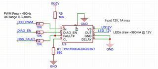
I have designed the following circuit to control a dumb LED strip's (just +12V and GND) power and brightness. The EN pin will be PWM'd in order to control brightness, and the switching frequency for that will be 490Hz. 

It will be getting a regulated 12V input at VS and it can supply 1A maximum. The LED strip will draw about 380mA maximum. Can you check the schematic to make sure it is designed correctly, will the supplied power be enough, and if I can use my desired PWM control scheme successfully on it?

Thank you in advance!

  • Hello, 

    The schematic looks good!

    For reverse current protection it is recommended that a blocking diode be added to VS as seen in figure below. 

    Another method used can be the GND network. This figure is also attached below.

    The recommended configuration is a 1-kΩ resistor in parallel with a >100-mA diode. The reverse current protection diode in the GND network forward voltage should be less than 0.6 V in any circumstances. In addition a minimum resistance of 4.7 K is recommended on the I/O pins. Note that if using a GND network which causes a level shift between the device GND and board GND, the CL pin must be connected to the device GND.

    What is the Duty Cycle of the PWM?

    BR, 

    Alan

  • Hi Alan,

    Thank you for the feedback, I will look into adding the diode at the VS pin. Is there an advantage of doing the GND network or the VS diode? It seems that the GND network adds some complications. I was planning to use the full range of 0-100% duty cycle for a "fade in" effect. Do you see any issues with using that range?

  • Hey, 

    Having the diode on VS will work fine in this application for reverse current protection. My concern with the ranging duty cycle would be giving the device enough on time for it to be properly enabled. I have attached the figure displaying the switching characteristics of the device. 

    With the Tdon/Tdoff and slew rate on/off the total time is around 200us. It would be best to ensure the duty cycle range will allow for this switching time. 

    Also you can reference this app note about driving PWM loads with TI HSS

    www.ti.com/.../slvaf10.pdf

    BR, 

    Alan

  • Hi Alan,

    I see. So if my calculations are correct, at a SF of 490Hz, a 1% duty cycle would give us a desired "on" time of 20.4us, which would be too fast. Then at minimum I would need to look into doing 10% duty at the lowest to have a visible "on" state, which would give us an on time of 204us. Is this the right thought?

  • Yes, that is the correct thought. I would provide a larger cushion for the on time and the duty cycle percentage. There will be power stressing during the PWM application that can increase the heat of the device in normal operation. If your application can operate 20-25% that's what I would recommend. 

    BR, 

    Alan