This thread has been locked.

If you have a related question, please click the "Ask a related question" button in the top right corner. The newly created question will be automatically linked to this question.

UCC21520: Question: I_VCCI quiescent supply current & supply power at VCCI =5V - 18V

Part Number: UCC21520

Tool/software:

Hi team,

Could you give me the imformation about the topic in question?

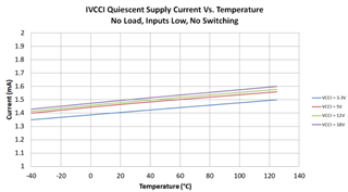
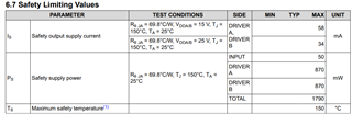
1. I_VCCI quiescent supply current at VCCI =5V - 18V

2. Supply power to INPUT SIDE at VCCI =5V - 18V

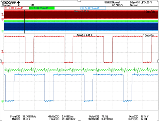
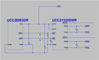
When I tested UCC21520DWR, VCCI - GND shorted.

Test Condition: 

VCCI=16V, VDDA-VSSA=16V, VDDB-VSSB=16V, INA=INB=16V(swiching frequency 20kHz-100kHz), VDT=VCCI

I suspect that INPUT SIDE supply power exceeded Safety supply power 50mW.

Please kindly advice if you find any doubt. Thanks.

Best Regards,

Iura

  • Hi Lura,

    Sorry for the very late response. There seems to have been an issue/bug with the thread assignments from our end. 

    I have some initial questions to better understand this:

    • Is the input PWM signal being inputted before powering up VCCI?
      • Important to keep in mind INA/INB absolute maximum specifications are a function of VCCI
      • Powering up INA/INB before VCCI exceeds the datasheet abs max specifications for INA/INB
    • Are there any waveforms you can share of the VCCI, INA, INB?
      • Interested to see if there is some significant noise levels seen there
    • If possible, would you be able to share the schematic?
      • This can help me check if there are any possible root causes from the schematic.

    Looking forward to hearing back!

    Regards,

    Hiroki

  • Dear Hiroki

    Thank you for your reply.

    >Are there any waveforms you can share of the VCCI, INA, INB?

    CH1:1(INA)-4(GND), CH2:3,8(VCCI)-4(GND), CH3:2(INB)-4(GND)
    I have not measured the waveform at the time of breakage.

    >If possible, would you be able to share the schematic?
    The connection diagram is outlined below.

  • Hi Iura,

    Thank you for following up with the additional details!

    CH1:1(INA)-4(GND), CH2:3,8(VCCI)-4(GND), CH3:2(INB)-4(GND)
    I have not measured the waveform at the time of breakage.

    It looks like there is not much noise on INA or INB and the transients in VCCI are well below the 20V absolute maximum specifications. From this waveform, there is nothing indicative of causing damage to the gate driver.

    Although you have not measured the waveform at the time of breakage, do you have any insight on the conditions under which the device failed?

    Here is a plot generated of the VCCI quiescent current across temperature at various VCCI voltage levels. There is not much of a difference at different voltage levels.

    Under switching conditions, if both channels are simultaneously on it will consume an extra 2mA of quiescent current. If complimentary, it will consume an extra 1mA of quiescent current. In your case with the example waveform, it will be approximately 1.5mA of extra quiescent current on top of the value seen on the generated plot.

    Regards,

    Hiroki

  • Dear Hiroki,

    In case that extra current is added to the quiescent current on Vcc=16V or more, is there a risk of damage by exceeding Safety supply input power 50mW?

    Regards,

    Iura

  • Hi Lura,

    The safety limiting values indicate how much short circuit current is required to damage the isolation capacitor. It is unlikely that the device will ever draw >10mA of continuous input current unless it is damaged. In the damaged condition, if you can limit the short circuit current below 10mA, you can protect your isolation capacitors and still maintain the full high-voltage isolation barrier. 

    Best regards,

    Sean

  • Dear Sean,

    Thank you for the reply.

    Does this mean that the safety limiting values are actually specified only in terms of current, not power?

    For example, with a quiescent current of 1.5 mA, an additional operating current of 1.5 mA, and VCCI = 17 V, the input power exceeds 50 mW defined as INPUT SIDE Ps.
    (1.5mA + 1.5mA) * 17V = 51mW
    Could this be a cause of failure?  Or is it OK because the input current is less than 10mA?

    Regards,

    Iura

  • Hi Iura,

    You are correct, the safety limiting values should be taking the supply voltage into consideration.

    In your example, it would be surpassing the safety limiting values for input side and would not be recommended for continuous use.

    Hope this answers your question.

    Regards,

    Hiroki

  • Hi Hiroki,

    In conclusion, I understood the following.

    - The VCCI input power must not exceed 50 mW.
    - Therefore, the additional input power must be reduced by lowering the duty ratios of INA and INB.

    Thank you for your help.

    Regards,

    Iura