This thread has been locked.

If you have a related question, please click the "Ask a related question" button in the top right corner. The newly created question will be automatically linked to this question.

UCC2897A: I AM HAVING ISSUE AT THE MAIN GATE PULSE WHERE I GET AUX BUT NOT MAIN GATE PULSE

Part Number: UCC2897A
Other Parts Discussed in Thread: PMP22495, , TL431

Tool/software:

Hello There

I am facing a issue in AC-DC using UCC2897A with reference to PMP22495 design. but here I didnt used Bootstrap Bias instead i use auxilary Bias for controller.

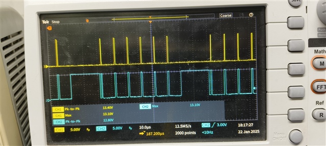
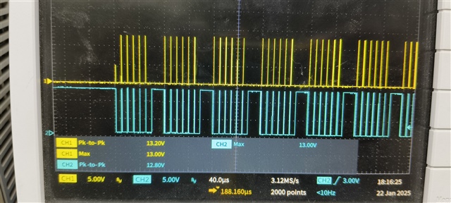
This is the waveform I am observing where the yellow is at the input of UCC5304D in PMP22495 which is AUXILARY AND THE blue one is at Gate of Main MOsfet.

HERE this application is made for 90VAC TO 264VAC.

AND I AM GOING TO GIVE THE CONTROLLERS 

THE SWITCHING FREQUENCY IS 100KHZ AND THE OUTPUT IS 15V/8A 

THE TRANSFORMER RATIO NP/NS IS 3.5 AND SAME RATIO FOR BIAS ALSO

RDEL IS 8.25K

RON IS 160K

ROFF IS 240K

RSLOPE IS 5K

VDD IS 1uF 

AS FOR BIAS WINDING VCC THE CAPACITOR IS 320 uF/50V

I AM GIVING VIN DIRECTLY FROM BULK VOLTAGE THROUGH A EMITTER FOLLOWER BASED LINEAR REGULATOR .

I THINK THE MAIN GATE PULSE IS TURNING OF QUICKLY BUT THE AUX PULSE IS FOR COMPLETE DUTY CYCLE.

KINDLY HELP ME SOLVE THESE.

THANK YOU

  • AND ONE MORE THING THAT IS IF THE VCC BIAS CAPACITOR IS VERY HIGH LIKE 320uF THEN WHAT IF THE TURN ON TAKES TOO MUCH OF TIME ?

  • Hi,

    The OUT and the AUX should have almost the same waveforms. So it looks the IC is damaged - you can change to a new IC to try.

    The damage can be from the OUT pin on your board shorted to ground. So check OUT pin to ground resistance before power on the IC to make sure no short.

  • Hi sir the Aux waveform is out of phase as in the PMP22495 an NMOS is used to invert the pulse . I observed the out pin isolating from main mosfet . the thing i observed is that the OUT IS ONLY FOR LESS DUTY BUT THE AUX IS FOR REMAINING 90% OF DUTY. AND I OBSERVED THREE CONSECUTIVE TRANGLES AT SS PIN GOING FROM 0 TO 2.5 AND BACK FROM 2.5 TO 0 AND AGAIN 0 TO 2.5 VOLTS.

    THE ISSUE IS NOT YET SOLVED BUT OBSERVED THIS THING

  • Hi,

    Please measure both AUX and OUT from UCC2897A so to find if UCC2897A works normal first.

  •  

    I MEASURED ITS JUST LIKE THE MAIN OUT PULSE below is of AUX AND ABOVE IS OF OUT.

    AS PER MY OBSERVATION EVEN THOUGH THE FREQUENCY SET IS 100KHZ THE AUX IS SHOWING 200KHZ INITIAL OR ITS SKIPPING ONE PULSE

    .AND IN SS PIN I AM GETTING TRIANGLE OR WAVEFORM GOING FROM 0.6 V TO 2.6V AND COMING DOWN FROM 2.6V TO 0.6V.

    KINDLY HELP.

    THANKS

  • Hi,

    UCC2897A OUT and AUX should have almost the same waveforms on the two pins. The IC looks damaged. You need to change to a new IC to check. Make sure no short or low resistance from OUT to ground 

  • FIND THE SCHEMATIC OF POWER STAGE ALSO

    THE YELLOW IS OUT AND BLUE IS AUX

    IT IS OBSERVED THROUGH 100VDC TO 380VDC .

    IT IS POWERED BY JFET .

    I WILL SHARE THE SCHEMATIC ALSO.

    IN THAT THE CIRCUIT NEAR THE DISABLE IS FOR HICCUP MODE FOR OUTPUT OVP.

    I HAD DISABLED ALL THE EXTERNAL PROTECTIONS FOR TESTING PURPOSE.

    I CHANGED THE GATE RESISTANCE TO 10E AND THE CBIAS TO 320uF.

    KINDLY HELP.


    AND THE PULSES ARE LIKE THESE EVEN FROM START UP.NOT LIKE ANY SPIKE ITS PURE SQUARE WAVE BUT OF VERY LESS DUTY CYCLE.

  • SCHEM.zip

    OPEN THE ZIP FOR SCHEMATIC HD IMAGE

  • Hi,

    Please provide the below waveforms of UCC2897A:

    CS pin

    FB pin

    VDD pin

    OUT pin

  • 0121.WAVEFORMS.zip

    HI THERE KINDLY FIND THE WAVEFORMS OF THE PINS OF THE POWERSTAGE WHERE YELLOW IS OUT AND BLUE IS RESPECTIVE PIN.

    BUT THE FB PIN IS 5V SAME AS VREF NO CHANGES IN IT DURING SWITCHING. 

    AND ONCE I HAD CHANGED THE IC AND ISOLATED IT FROM OTHER CIRCUIT EXCEPT RON ROFF RDEL RSLOPE VDD CAP VREF CAP SSCAP AND RF Ccs Rcs. with all these i turned on the FRESH NEW IC . I HAD EXTERNALLY GIVEN 1.3VOLTS AT LINEUV PIN, AND GROUNDED LINEOV PIN. AND USED ISOLATED 15VOLTS PSU FOR VDD.

    BUT NO IMPROVEMENTS I AM GETTING SAME PULSE OF 200ns.

    KINDLY HELP .

    I ASSUME THAT MAY BE THERE IS ANY ISSUE WITH RSLOPE OR CS.

    AND THE OUTPUT VOLTAGE IS 15V AND Lo = 68uH. TRANSFORMER IS Np=21,Ns=6,Nb=6 frequency is 100khz. transformer primary inductance is 1.54mH. DUTY AS PER RON IS 0.6.

    KINDLY USE THE ABOVE DATA AND HOPE IT WILL HELP IN SORTING OUT THE PROBLEM.

    THANKS WILL BE WAITING FOR YOUR ASSISTANCE.

  • FIND THE SCHEMATIC OF POWER STAGE ALSO

    THE YELLOW IS OUT AND BLUE IS AUX

    IT IS OBSERVED THROUGH 100VDC TO 380VDC .

    IT IS POWERED BY EXTERNAL BJT . BASED LINEAR REGULATOR FOR START UP

    I WILL SHARE THE SCHEMATIC ALSO.

    IN THAT THE CIRCUIT NEAR THE DISABLE IS FOR HICCUP MODE FOR OUTPUT OVP.

    I HAD DISABLED ALL THE EXTERNAL PROTECTIONS FOR TESTING PURPOSE.

    I CHANGED THE GATE RESISTANCE TO 10E AND THE CBIAS TO 320uF.

    KINDLY HELP.


    AND THE PULSES ARE LIKE THESE EVEN FROM START UP.NOT LIKE ANY SPIKE ITS PURE SQUARE WAVE BUT OF VERY LESS DUTY CYCLE.

    HERE

  • Hi,

    Based on your CS and OUT waveforms, the CS has very high noise and it looks the CS noise turning off OUT. So you need to reduce the noise.  You can increase C26 from 100pF to be bigger, up to 1nF to see if the CS noise can be reduced or OUT pulse can be wider.

    Please provide board layout for reveiw as well. 

    The VDD looks up and down. To help debugging, you can temporary use an external voltage source with 14V and a diode to connect to VDD pin to avoid this up and down so allow you to check other behaviors of the converter.

  • I had used external source after this. but no changes.

    I think the ss is not going above 2.5 means ss pin is discharging as soon as the OUT is ON.

    What are the conditions that force the SS to discharge.

    Can you explain The Enable of UVLO and SS.

    I will check with increasing Ccs and inform you.

    I actually set a new bord with only control circuitry with no feed back and only Rcs. But it's coming same. Is there ? Anything related to slope compensation?

  • Hi,

    Yes, get CS noise lower first then send me the waveforms of these CS, VDD, VREF, OUT, FB.

  • waveforms2.zip

    I FOUND THE ISSUE, IT WAS WITH THE LINE UV PIN DUE TO NOISE. I ADDED 47nF ACROSS THE GROUND RESISTOR.

    NOW QUITE IMPROVE MENT. BUT WITHOUT CONNECTING THE OUT TO MOSFET THE PULSES ARE GOOD BUT AFTER CONNECTING. IF YOU SEE THE WAVEFORM NAMED VDS AND GATE THERE EXISTS NOISE IN THE VDS AND ALSO THE GATE WIDTH IS NOT MUCH. I AM ATTACHING THE MOSFET DATASHEET. KINDLY GO THROUGH IT AND BASED ON SCHEMATIC. SUGGEST ME WHAT HAS TO BE DONE.

    SORRY THE PIC WITH VDS AND GATE IS ACTUALLY ONLY VDS . THE OTHER IS THE SWITCHING NOISE NOT THE GATE SIGNAL.

    THE CBIAS IS 320uF. AND THE INPUT VOLTAGE IS 120VDC.

    VDD IS SAME LIKE RAMP VREF IS LIKE SQUARE WAVE.

    AND FB IS SAME AS VREF. BECAUSE AT OUTPUT NO VOLTAGE.

    WITH CS I WILL CHECK. BUT THE GATE IS NOT GOOD . AFTER CORRECTING THIS I WILL SHARE. THANKS

    KINDLY LET ME KNOW WHAT TO DO NEXT.

    THE MAIN MOSFET DATASHEET :  infineon.com/dgdl/Infineon-IPT60R105CFD7-DataSheet-v02_01-EN.pdf?fileId=5546d46271bf4f920171df2a7e5530ef

  • Hi,

    Please provide CS waveform along with OUT waveform. I suspect CS noise caused the difference.

  • OK I WILL PROVIDE TOMORROW. BUT WHAY IS THAT SPIKE IN BETWEEN THE DRAIN WAVEFORM WHILE IT IS ON. 

  • Hi,

    I am not sure why GATE waveform like that, you need to check from OUT pin waveform and CS pin waveform to help understand why GATE waveform is like that.

  • Hi Mr. Hong.

    thanks a lot for your help. I found that issue was with the grounds. the cs ground and the LINEUV / UV grounds was to be on signal ground but it was connected to power ground thus noise.

    I changed the grounds from pgnd to gnd. now I get continous pulses. but now new kind of issue are found. those are the out put once turned on takes nearly 3 secs to go from zero to 15V . and as i apply load the voltage drops kindly help me with the issue i will attach the fb pin waveform along with drain thanks.

    attached the feed back and the compensation RCOMP IS 39K AND Ccomp is 1nF AND Cz is 100pf. kindly help me with the issue regarding the outpu voltage.

  • Hi,

    No attachment as you mentioned of feedback. 

    Did you check soft start, and VDD waveforms to find the 3 seconds are due to VDD rinsing, soft start or something. You need to capture SS, VDD and OUT waveforms to see when OUT start to show pulses.

  • The waveform I sent in previous reply is feedback. I will share the waveforms of SS, VDD and OUT. Another thing is when ever I put 1A of Load it goes from 2 V to 15V and takes nearly 3 secs to stable. Is this anything related to compensation?

    Because Css is 0.1uF that's it

  • Hi,

    Please provide the waveforms of CS, VDD, FB, during time you change load.

  • Hi,

    Please label which one is FB CS VDD

  • yellow is VDS 

    BLUE IS FB

    i found that the  delay rise was due to compensation. i changed the compensation to Rcomp to 51K AND Ccomp to 47nf AND Cpole to 100pf  and then i changed the resistor paralle to optocoupler which biases Tl431 from 10k to 1 k.

    and now the RF is 2.2k and Ccs is 220pf and Rslope is 180k

    now the pulses are continuous. and output is stable. at 15V 

    but now I am getting new issue,normally now I am doing testing with input 100Vac  but as i increase and go to 230Vac its working. but if i turn on at 230Vac It goes some kind of protection and drain peak is double the input.

    I am sharing the drain waveforms. 

    THE Ccl is 22nf.  

  • Hi,

    I am not understanding your description can you clarify:

    - when power on at 100Vac, the converter doesn’t work until you increase the voltage to 230Vac then the converter works normal - is is what you want say?

  • No , when I apply 100VAc the converter starts working. But when I apply 230 and turn the switch on the converter goes to some kind of protection.But if I turnon the switch at 100VAc and then If I increase to 230 using a variac. At that even at 230Vac also its working. But if you apply 230 Vac directly and turn it on its not working.

  • Hi,

    When you apply 230Vac at power on, please provide the waveforms of the below in order to help find why 230Vac power on shows protection and which protection(s) is triggered. Without the below waveforms it is not able to help to find the reason.

    CS pin

    FB pin

    VDD pin

    OUT pin

    SS pin