This thread has been locked.

If you have a related question, please click the "Ask a related question" button in the top right corner. The newly created question will be automatically linked to this question.

TPS4811-Q1: SOA calculator questions

Part Number: TPS4811-Q1

Tool/software:

Hi,

while working with the SOA calculation sheet some questions emeregedwhich hopefully you can answer me:

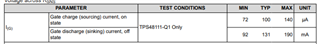
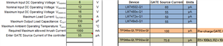
  1. Where does the recommended value for the "gate source current" (75,6uA in case of the TPS4811) come from?
  2. How does it change when varying the gate resistor R1 (~100k) and what is it dependedn from?
  3. What should i enter in, for example, F55 (1ms SOA Current @ VIN(MAX)) if the voltage is already outside the SOA? It doesn't let me enter 0A, so i resided to 0.0..01, which worked fine

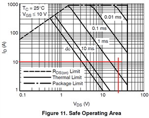
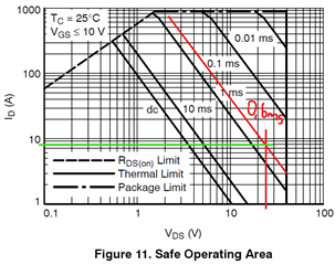
  4. How do I work with the SOA graphic of the MOSFET if neither the current through nor the voltage over the MOSFET are linear/constant?
    If read the application note SLUOOA2 regarding the SOA but it wassn't really applicable in my case, at least I didn't see how.
    Can I just integrate the power of the FET during turn-on over time and find an approximation using a square wave with the same energy integral?

    I can't imagine this a good starting point, because since, at least simplified, E = U x I x t gives me 3 variables to play around, I can achieve many very different operating points while keeping the energy constant.
    Or do I use the worst case V_DS and I_DS over time (like in the application note) and adjust just the time to achieve a pulse with equivalente energy?

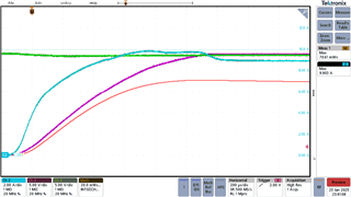
I will add an oscilloscope measurement afterwards.
Currently, I'm using a NTMFS5C410N from onsemi as MOSFET in a 24V system.
Probably I will switch over to a FET with 60V/80V V_DS to have a higher margin.

  • Furthermore, what is "Required Maximum allowed Inrush Current" dependend on? I understand it like this: The maximum current that can pass through all traces and components in the path without destroying something, e.g. traces, current sensors, resistors, CMC or other filter components, etc.

  • Now the aformentioned oscilloscope picture:

    Blue: I_D
    Green: V_D
    Purple: V_S
    Red/Orange: E_FET (Integration of ((V_D-V_S)*I_D)

    Peak energy is 70,6mJ with V_DS,max = 24 and I_D,max = 9.9A -> t = 70,6m/24V/9.9A = 297 us ~ 0.3 ms

    SOA of the NTMFS5C410N

  • Hi Lukas, 

    1. The Gate Source current is in the electrical characteristic table of the datasheet and listed directly to the right in the calcualtor:
    2. R1 will change the INRUSH current of the device. The expectation is for the calcualtor you use the max allowed INRUSH and design R1 to meet that.
      1. See section "8.3.2.1 FET Gate Slew Rate Control" of the datasheet and use equations (2) and (3)
    3. For 10 ms SOA current @ Vin(MAX): if your voltage is already exceeding the FET SOA then you probably need to choose a different FET. Vin MAX should be the max deviation of your operating voltage. For example, if you expect VBATT to be 12V nominal maybe 16 V is the maximum. The FET must handle this. The field F55 is for the load current expected at that voltage. 
    4. Typically the FET SOA calcualtor is only used for start up conditions. Primarily you need to make sure the INRUSH will work with the FETs chosen. 
    5. The INRUSH description is correct. The FET will have parameters that indicate required maximum currents. Slew rate controls like R1 mentioned can help control this. 

    To further help consider this app note and below steps for calculating the FET SOA. 

    FET SOA stress calculation

    A more detailed explanation of SOA calculation is specified in section 2.3 Understanding MOSFET’s Stress Limitations of Robust Hot Swap Design App note.

    For your understanding below is a step by step procedure (extracted from the app note),

    1. Calculate the power stress on the FET during startup. Refer to section ‘2.3.3 Checking SOA for Non-Square Power Pulses’ of the app note.

    Derive t2. Approximation here is  that the FET is stressed for a power loss = P2 = PMAX for t2 duration.

    1. Now, estimate SOA the FET can handle for t2 This value will be at room temperature. Refer to section ‘2.3.2 Checking SOA for Intermediate Time Intervals’ of the app note.

    Remember that the SOA value in the table below needs to be taken at VDS = VIN(max) in the SOA curve of the FET.

    1. Now, De-rate the SOA calculated in the above step for the Max operating junction/ case temperature of the FET. Refer to section ‘2.3.1 MOSFET SOA Curve and Thermal Model’ of the app note.

    This value can be taken as the temp. of the FET at max load condition,

    1. You can consider that the FET has strong SOA if

    SOA(TC) > 1.2 x (P2 / VDS)

    Where,

    SOA(Tc) is from step 3

    P2 is from step 1

    VDS = VIN(max)

    The factor 1.2 is taken to include a 20% margin.

    Thank you, 

    Sarah

  • Hello again,
    thanks for the extensive answers, but some of my questions were a bit misleading I suppose:

    1. I have found both a. and b., my questions was intended to be: Why are a and b not the same?
      Were do the 75,6uA from the calculator come from.
    2. With this question I intended how a different gate resistor R1 changes the gate source current, not the I_D inrush current.
      Do have to adjust it if I use values other than 100k and if yes, in which way?
      If I would use 200k for example, do I get half the current only or does it stay the same or is there another formula?
    3. You wrote F55 is for the "expected" load current at this voltage. With this you intend the maximum possible load current (taken from the SOA graphic) and not the real maximum possible voltage, right? The "expected" part in your answer confuses me a bit.
      Would you reccomend to change the FET even though I expect the turn-on time never to be higher than 1ms? 
    4. + 5. Understood!

    Continuing the example above I measured a Pmax of 116W.

    Using the formula i get a t2 = E_FET/P_MAX = 608us -> inserting this timing in the SOA graphic and using V_IN = 24 as V_DS
    I get a current of I_SOA(25°C)=8A

    Accounting for derating that gives me a I_SOA(85°C) = 8A * (175-85)/(175-25) = 4,8A

    Concluding, I_SOA(85°C) > 1.2 * (P_MAX/V_DS) = 1.2*(116/24) = 5,8A is not complied with.

    Could you confirm this calculation is correct that far?

    Possible solutions would no be to either

    1. decreas the turn-on time (R1) since a higher inrush current wouldn't bother the FET or other components
    2. use a FET with a wider SOA

    Thank you very much for your help!

    Lukas

  • Hi Lukas, 

    1. I see. The 100 uA is specific to the TPS48111 device. The 75.6 uA is for the other  variants. Let me pin point the exact number. 
    2. So the resistor at the gate does limit the source current. Typically what I would recommend is to use the capacitor charging equation to solve for I. (C = I* dv/dt), from here you can consider what R1 is using the initial startup voltage at the gate, which would be ~12V. (12V/ I = R1).
    3. Yes. I think the field represents the SOA current specific to the FET but at the max voltage you are setting (since that's what the FET will see across the DRN-SRC). As far as changing the FET its up to you. We are trying tor provide tools to help customer develop their system. If you are confident that 10ms of sustained failure isnt an issue for you then you could keep the FET choice. 

    Yes your calculation seems correct. as does your second solution. If the higher INRUSH current inst an issue that is also viable. 

    Thank you, 

    Sarah

  • Hello Sarah,

    thanks again for your answer and confirming my way of calculating the SOA.

    One last question from my side still remains about your answers 1. and 2.

    What can I use for dv/dt at the gate if I'm still in process of designing my circuit or is it a IC intrinsic value?
    Otherwise I see no other way than assuming 12V and a completly empty capacitor at startup -> assuming a short-circuit as capacitor on startup.

    In this case the peak current would be 12V/100k = 120uA, but quickly dropping to around the leakage current of the FET/capacitor after charging the gate/soft-start capacitor to 12V. But I still don't understand in this case where the 100uA are coming from and even less the 75.6 uA. It's strange because in the datasheet are only ever mentioned the 100uA for gate and precharge gate (in case of the TPS48111). I'm also fairly certain that the 100uA value in the SOA margin calculator refers to the precharge gate, at least according to my understanding.

    Thank you if you could clearify als this last point! regarding the rest I'm very grateful for your helpful answers!

    Lukas

  • Hi Lukas, 

    Dv = V_BST (12V) – Vg,th (3V typ) = 9V ; where Vg, th is of the FET chosen

    dt = turn on time you want (ex. 10 us)

    The 120 uA would be the current you are limiting the gate to. And yes I am trying to clarify internally where the 75.6 uA can be found, but I think its safe to consider both in your calculations and see how different they are. It should still get you very close to selecting the correct FET. 

    Thank you,

    Sarah