Other Parts Discussed in Thread: UCC27714
Tool/software:
Hello,
I would like to develop a charger for LiIon battery packs with 12S, i.e. 50.4V max. I want to charge them with up to 20A and and 48V input voltage.
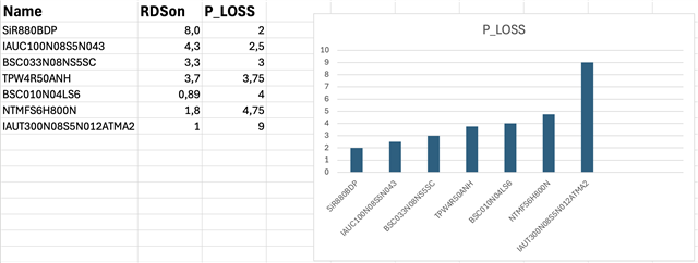
I designed a custom PCB for this purpose using the BQ25756. Testing the design showed, that the inductor (Würth Elektronik 74435580680) and the Mosfets (Vishay SIR880BDP-T1-RE3) get rather hot. Charging with only 3A gets the Mosfets to about 55-60°C. Charging with 6A lead to extremely high temps in the inductor of about 170°C measured directly on the windings, and rising. Also high temps on the mosfets of about 110°C. These tests even included some small heatsinks and a fan for cooling the components. As the Inductor is supposed to have a DCR of 2.1 mOhm, I was not expecting thermals like this.
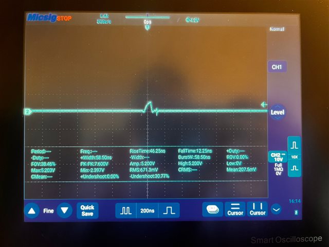
Attached you can find a picture of my oscilloscope. X axis spacing is 1us/div. It shows the voltage across the inductor at 3A charging current. Input was 48V, V_BATT was 46.5V.
Can somebody tell me if this behaviour is expected? If yes, what could be done, to drastically improve the performance, so I will be able to charge with 20A?
Thanks,
Max


 This is LODRV1.
 This is HIDRV1.
 This is LODRV2.
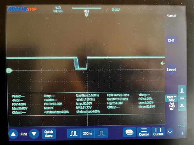 BTST1 2A 450kHz
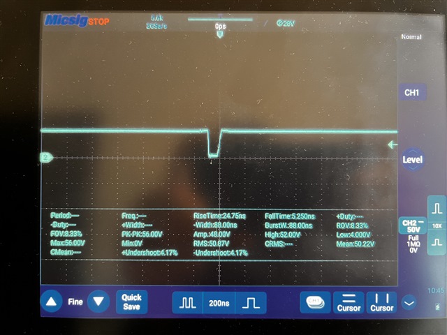 BTST2 2A 450kHz
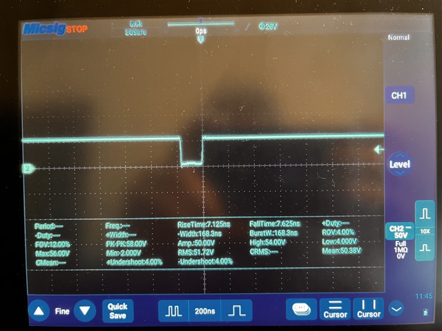 BTST1 7A 300kHz
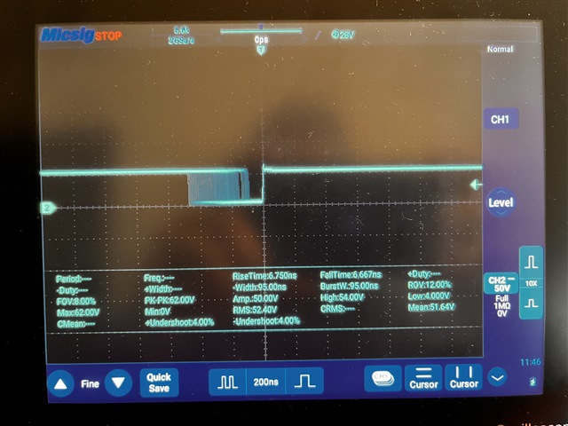 BTST2 7A 300kHz
 LODRV1 5A 300kHz with internal 5V at DRV_SUP
 LODRV2 5A 300kHz with internal 5V at DRV_SUP
 internal 5V DRV_SUP at 5A
 LODRV1 5A 300kHz with external 7V at DRV_SUP
 external 7V DRV_SUP at 5A (KORAD KWR103 PSU)
 LODRV1 7A 300kHz with external 7V at DRV_SUP
 external 7V DRV_SUP at 7A (KORAD KWR103 PSU)