This thread has been locked.

If you have a related question, please click the "Ask a related question" button in the top right corner. The newly created question will be automatically linked to this question.

LM5122-Q1: Need Help with 3A 100V design on LM5122

Part Number: LM5122-Q1
Other Parts Discussed in Thread: LM5122

Tool/software:

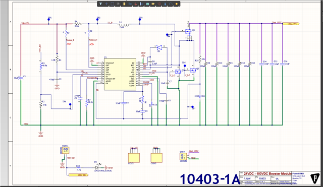
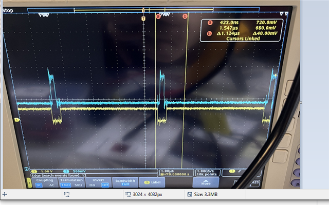
Hi, I am currently working on a design I created using Webench Power Designer am finding that my FET and the LM5122 is not surviving. It looks like the SW pin is sinking too much current and burning up. I am using the IRFR4620TRLPBF N-MOSFET for my Low side switching and a BSC160N15NS5ATMA1 N-MOSFET for my high side. 

My question is why is my IC and FET failing under the current design?

  • Hello Joseph,

    Thanks for using the e2e forum.
    I am sorry you to hear your LM5122 design is malfunctioning.

    Would it be possible to provide the following information:
    - Input voltage range
    - Output voltage
    - Max output current
    - Which components are taking damage? (low side FET, high side FET, IC itself?)
    - Schematic of the design for review

    Thanks and best regards,
    Niklas

  • Also, can you confirm if the applications only breaks at higher loads, or at light load conditions as well?
    If you have any waveforms available that show the switch node signal during normal operation, it would be helpful as well.

    Thanks and regards,
    Niklas

  • Hi yes here is my schematic to start off: 

    Input voltage range is supposed to be 21V to 27V

    output voltage is supposed to be 100V

    Max current is supposed to be 3A

    I found my low side FET was failing and I believe it was not rated for the power I wat switching it with, so I switched to a higher power FET and it did not break. 

    After added the higher power low side fet I was getting 99.7V at the output. I then loaded the booter with 66Ohms of resistance and the voltage dropped to 60V at the output. Not sure why this is happening. My new question is why is this happening?

    Here are my switching output waveforms. They are quite noisy: 

  • Hi Joseph,

    Thanks for all this data.
    An output voltage of 100V is very close to the abs max limits of the LM5122 device.
    The SW pin is rated for 105V, meaning a 10% overshoot on the switch note could be enough to break the IC.
    As you already commented yourself, the MOSFETs need to support the same voltage levels.
    For confirmation, you can measure the Vgs voltage at the low side FET during operation to check if the peak voltage goes above 105V.

    To work around this limitation, it might be required to use external drivers with higher voltage ratings in combination with the LM5122 device.

    Best regards,
    Niklas

  • Thank you for the feedback. Do you have any example circuit topology of how I can implement external drivers for this design without reaching the voltage limit of the IC? 

  • Hi Joseph,

    Unfortunately, I did not find a reference design that does match your specs.
    The closest input/output parameter match was with a SEPIC design, where LM5122 is used asynchronous, meaning SW pin is connected GND and diodes are used instead of the high side MOSFET.
    https://www.ti.com/tool/PMP23320

    However, I did see customer designs which use LM5122 in regular boost topology together with these external drivers:
    https://www.ti.com/product/de-de/UCC27211
    These are rated for 120V.

    Best regards,
    Niklas