A related question is a question created from another question. When the related question is created, it will be automatically linked to the original question.
If you have a related question, please click the "Ask a related question" button in the top right corner. The newly created question will be automatically linked to this question.
sure we can review the schematic. Please share it together with the filled out LM5176 Design Calculator to this thread? This would be the most efficient workflow for us to do a schematic review.
the most efficient way and fastest way is the E2E forum as this gets tracked and maintained daily by the team - so e.g. even if I am out of office you would get a reply
If you worried about putting your data in the forum, you can send this via private message (hover the mouse over my name and select private message.
In this case please also drop a note here that you have sent a private message.
(In below list items which should be checked again have been marked bold) (Note: other info are left here to give an overview of what has been checked)
Quickstart Calculator:
Slope compensation capacitor is much lower then recommended
Full load at lowest VIN will not be possible as the losses are getting very high
Schematic:
Series Resistor with 2k at VISNS (required if Vin > 40V but recommended for all conditions as VIN can also go higher during bursts, only LM5176)
BIAS connected If BIAS is not used connect to GND or VIN (do not keep open) - BIAS max = 40V !
MODE: allowed Resistor (LM34936 only 93k1 or 200k or Vcc)
Cap at VCC Cap at VCC large enough - check ratio to Boot Caps (at least 5)
Cap at EN/UVLO Adding a Cap to the low side resistor of the EN/UVLO can help to avoid ripple in startup esp. of very low startup voltage is selected
Snubber on SW1 and SW2 (or Schottky diode ) Place Footprint for a snubber at SW1 and SW2 (they can then be populated in case needed (e.g. due to EMI) without layout change) Note: Snubber Resistor connected to GND not Inductor for better Thermal performance
Snubber connected to PGND not to Sense Resistor -> do not connect to Sense resistor to avoid snubber current injection into Sense signal
Add Series Resistor into MOSFET Gate signals lines (they can then be replaced in case needed (e.g. due to EMI) without layout change, additional option: add a diode in parallel for slow on and fast off.
Gate resistors are <=5 Ohm
Voltage rating of MOSFET (Have a margin of 30% is recommended)
Use Kelvin connection for Current Sense (CS/CSG) to LM5176
UVLO setting relative to lowest input voltage
Select the suggested capacitor for slope compensation. Preferable next lower instead of higher value (= more slope compensation)
Please check phase margin over the full range (recommend > 60 Degree)
Layout checklist (for you reference only )
(In below list items which should be checked again have been marked bold)
Vcc Cap close to pins
AGND and PGND connected at Thermal pad - yes
Via's in Thermal pad: Thermal Pad could get more via's to better distribute power loss of the LM5176
AGND island -> a AGND power area help to avoid disturbances injected into the AGND related components
Kelvin connection to CS/CSG sense resistor -> CSG should have dedicated wire to sense resistor not via ground plane
Kelvin connection to ISNS+/- sense resistor (shorted to GND if not used)
Small current loop for HDRV1/SW1 (area enclose by this wires should be as small as possible - best to have both on top of each other)
Small current loop for HDRV2/SW2 (area enclose by this wires should be as small as possible - best to have both on top of each other)
Input caps close to MOSFET
Output caps close to MOSFET
FB divider close to LM517x
PDF link: HTML links: Additional info on layout can be found here :
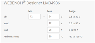
as you see from the calculation sheet the recommended sense resistor is 1.7mOhm while you selected 3mOhm. So controller might detect overcurrent already to early.
I am also concerned about the losses. This show already losses of > 10 Watt for higher currents which would be a temp increase of 200 Degree.
For lower input voltages even more.
Same for the inductor loss.
For that output power level you either would need active cooling or a multiphase design.
FYI, The schematic can not be accessed anymore - link expired
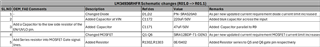
From the change list and the last recommendation following items seems not to be reflected:
Snubber connected to PGND not to Sense Resistor -> do not connect to Sense resistor to avoid snubber current injection into Sense signal
Slope compensation capacitor is much lower then recommended
To your questions:
1. output power: this is not limited by the controller but by the external components, e.g. inductor, MOSFETs,.... and also the thermal conduction of the PCB.