This thread has been locked.

If you have a related question, please click the "Ask a related question" button in the top right corner. The newly created question will be automatically linked to this question.

TPS22810: TPS22810 Enable

Part Number: TPS22810

Tool/software:

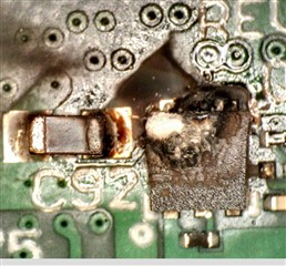
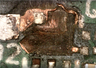
I am seeing a failure mode on the enable pin of the TPS22810 melting and the TPS22810 packaging melting during normal operation with Vin=12V. The datasheet specifically calls out that the enable can be driven by a 1.8V, 3.3V or 5V GPIO on page 15, but the recommended operating conditions for Ven Min/Max are 0-18V. In our system we tie the enable directly to Vin and Vin=8-15V. In the failure mode the system is running at 12V in normal steady state condition and the TPS22810 spontaneously fries. The steady state draw of the system is 250mA current. Can you verify that the enable pin can handle being shorted to the VIN with 12V-15V?

  • Thermal vias were not used underneath the IC. As the junction-to-ambient temperature is massively different between the DRV (currently using) and DBV packaging is there any data between thermal via and no thermal vias to estimate the thermal junction I might be reaching? 

  • Hi Dan,

    The device have thermal shutdown functionality so that should have protected the device if the issue was only due to junction temperature.

    Just want to check, did you do any other tests or are you very familiar with the device. 

     First thing I would say is can you check soldering and see if there are any shorts?. Also use multimeter diode mode to check diode drop from GND to all pins. We should have ESD structures which should provide some diode drop. 

    Next, if possible, check if you can use external EN signal to verify if the system is getting damaged or not. Ideally EN should not draw much current also. 

    These steps will help in isolating the issue. By any chance, do you have TI EVM for this device?

    Best Regards,
    Arush

  • We do not have a TI EVM for this device. We have this device on multiple designs across many units but only seen the failure mode two times so far. These units operated without issue for extended periods of time before they failed. Inrush current is measured to be 1.2A. 

    Since the result of the failure is that the TPS22810 overheats and melts I cannot measure the faulty ICs. We will be testing running 3A-4A continuously through the device and see if we can get a similar failure mode.  

  • I've been able to continuously draw 3.5A from the IC for hours without issue on our board. Our max usage at startup would be limited to 1.2A. Likely causes seem to be infant mortality on this IC, Thermal protection failure on IC, or flux residue underneath the IC eroding the PCB. Can you provide any data on any of these issues being present historically? 

  • Hi Dan,

    We don't usually see these type of early fails since all our parts go through ATE and will gets scrapped if they fail the ATE. We have FIT rate calculator on our website. 

    I think this issue is most likely caused by board short or soldering short. On the board with damaged IC, do you see any damage to traces. If it is still working, can you replace the device with a fresh device and test (multimeter and startup) to see if you find any board level issue. 

    Best Regards,
    Arush 

  • That is helpful info. So the ATE has coverage for the thermal protection circuitry? 

  • Hi Dan,

    Yes, I am expecting ATE to cover this. I am still double checking this with the test engineer.

    Best Regards,
    Arush

  • Hi Dan,

    I am following up with the engineer and am expecting to get back to you by today eod.

    Best Regards,
    Arush

  • Hi Dan,

    I checked with the test team. We are not checking Thermal shutdown for this part during production testing. Thermal shutdown is guaranteed by design in this part. 

    I think this issue is most likely caused by board short or soldering short. On the board with damaged IC, do you see any damage to traces. If it is still working, can you replace the device with a fresh device and test (multimeter and startup) to see if you find any board level issue. 

    Any update on this?

    Best Regards,
    Arush

  • I see. Thank you for the info. Unfortunately, on these boards we are not able to recover them as the failure mode results in the IC disintegrating and melting through multiple layers of the circuit board directly under the IC. The boards after have a short between power input and ground due to the melting of the dielectrics. 

  • Hi Dan,

    Understood. If you have any fresh boards remaining, can you check this. No need to power on the device. Just check this after soldering the device. Also can you share some photo of damaged device (while it is still on the board). Just send zoomed in board to prevent sharing full design.

     First thing I would say is can you check soldering and see if there are any shorts?. Also use multimeter diode mode to check diode drop from GND to all pins. We should have ESD structures which should provide some diode drop. 

    Best Regards,
    Arush

  • On a functioning board there is a 500mV-700mV diode drop from ground to the other pins and no shorts to ground. The damaged IC can be seen on the left and with it removed and the debris pulled off the plane below that has been melted through and now is shorted to the power input. The failure is identical on two boards. 

  • Hi Dan,

    Thank you for the update.

    Since this is also not repeatable, I am not sure what to suggest at this point. Do you have any specific questions which I can answer. 

    Best Regards,
    Arush

  • I understand. You've been very helpful. Thank you for the info. I'll mark the issue as resolved.