This thread has been locked.

If you have a related question, please click the "Ask a related question" button in the top right corner. The newly created question will be automatically linked to this question.

TPS60400-Q1: TPS60400Q burned

Part Number: TPS60400-Q1

Tool/software:

Hello,

I have the following circuit:

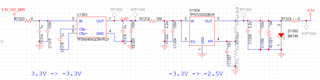
This circuit creates stable -2.5V from +3.3V by using charge pump from +3.3V to -3.3V and then negative LDO from -3.3V to -2.5V.

The maximum load of the -2.5V is 0.5mA (So the input voltage of the negative LDO is -3.25V (-3.3V + 100ohm*0.5mA), and the negative LDO needs voltage of at least -2.7V so its ok).

i had a problem in 2 boards (from 30 boards that doesn't have this problem) that the charge pump TPS60400Q was burned.

I did 2 experiments:

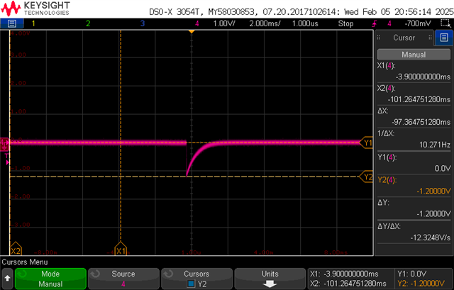
1. I shorted the -2.5V to ground for a couple of minutes and saw 19mA DC output current from the charge pump (The maximum allowed output current of the charge pump is 60mA). Than i released the short and the -2.5V came back.

2. I connected the 3.3V power supply directly to the input of the charge pump and saw current spike of 25mA on the 100 ohm resistor (output of the charge pump). The maximum allowed output current of the charge pump is 60mA.

I don't know what caused this problem. Also i tested this circuit in -40C and +80C and didn't saw any issues.

Do you see any issues in my design?

Thank you

Maor M.

  • Hi,

    The input voltage of the charge pump can turn on or off with series switch by MCU command.

    When i turn off the input voltage i see current spike of 12mA from the LDO to the output of the charge pump.

    I don't know if this is what caused the issue.

  • Hello,

    I will review and get back to you tomorrow.

    Thanks,

    Febin

  • Hello,

    A few clarifications:

    1. From your description, your experiments burned the charge pump but not the LDO by shorting the output of the LDO. Is that correct?

    2. 

    connected the 3.3V power supply directly to the input of the charge pump and saw current spike of 25mA on the 100 ohm resistor (output of the charge pump). The maximum allowed output current of the charge pump is 60mA.

    When you directly connect the power supply, can you add additional input caps and try again?

    3. 

    Also i tested this circuit in -40C and +80C and didn't saw any issues.

    What do you mean? The problem is only at room temp?

    4. I am a little confused. Did shorting the LDO output or direct power supply or turning off the input voltage through MCU command burn the device? Or all 3 burned the device?

    5. Can you share the Vin, Vout and Load scope plots for the charge pump?

    6. Did you test all 3 scenarios on all 30 Boards?

    Thanks,

    Febin

  • Hi Febi,

    1. No, i will summerize:

    In the start i had 1 board. Then i tested this circuit with the following tests:

    Voltages readings, ripple, short circuit of the -2.5V, load the -2.5V at 5mA, inrush current at the output of the charge pump to see its no more than 60mA. Then i reapeted all these tests at oven at -40C and 80C.

    After i saw all the tests were ok i approved this board.

    Then we manufactured 30 more boards and in 2 of them the charge pump burned during operation in the system.

    Then i took 1 board to investigate the issue and i did all the tests i described to you at the first message to see if i can burn the charge pump in this board but i didn't succeed to burn it after all the tests i did.

    2. There are already a lot of capacitors at the input of the charge pump in another places in the board. The 1uF input capacitor in the picture is close to the charge pump.

    3. See the explanation at section 1.

    The problem on the 2 boards caused at room temperature.

    4. I don't know exactly what caused the burning of the charge pump because the boards were assembled on systems and another people worked on these systems. I just know that they replaced the charge pump and the board worked after that. So there was no short circuit at the -2.5V. Maybe they turned off the input voltage of the charge pump by MCU command.

    5. Yes, i will check it on Sunday when i will come to work.

    6. No, i tested the scenarios at the first message only at the board i took for the issue investigation after the burning of the two charge pumps.

    When I measured the two burned charge pumps i saw short between the input and the output ( not from the gnd to the input and not from the gnd to the output).

    Note: the 100 ohm resistor is meant to limit the output current of the charge pump during startup so it will not exceed the 60mA.

    Thank you

    Maor M.

  • Hello,

    Honestly, I cannot say what have caused this problem.

    But I would suggest to track down the exact event that burned the device and we can take it from there. Please only make one change at a time and please record scope plots as I mentioned above.

    When I measured the two burned charge pumps i saw short between the input and the output ( not from the gnd to the input and not from the gnd to the output).

    Another thought, could anything go wrong during manufacturing? 

    Thanks,

    Febin

  • Hi Febin,

    Do you see any issue with the design from the first picture?

    Thank you 

  • Hello Maor,

    Do you see any issue with the design from the first picture?

    For the CP, everything looks fine.

    Thanks,

    Febin