This thread has been locked.

If you have a related question, please click the "Ask a related question" button in the top right corner. The newly created question will be automatically linked to this question.

LM2679: LM2679S-ADJ/NOPB Model Load Current Problem

Part Number: LM2679

Tool/software:

Hi, I am making a converter with my university graduation work. 

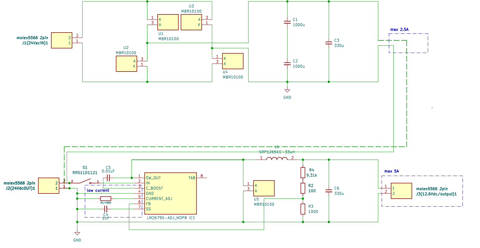
I'm designing a buck converter that takes 24Vac voltage as input and outputs 12.6V dc voltage.

It was designed as shown in the circuit diagram in the figure, and it was confirmed that the output voltage came out normally under no load.

However, when a resistance load of about 5 ohms was connected, the DC voltage gradually increased and applied to J2, and the actual current flowed by about 2.36 A, and the current suddenly decreased when it exceeded that.

According to my opinion, even if the input voltage increases, it should be fixed at 12.6 V and 2.5 A should flow continuously.

I designed the circuit by referring to the data sheet. I tried various things to solve this problem.

I tried to lower the current limit resistance on pin 5 and modified the output capacitor value.

And I also didn't use the soft start function. But I couldn't solve it. So I left an inquiry like this.

Thank you for reading the long text and I will attach the experimental video and photos in the circuit diagram. Your response would be greatly appreciated. Have a nice day

Thank you for reading the long text and I will attach the experimental video and photos in the circuit diagram.

If there is any waveform or information you need, I will let you know right away.

I would like to see and ask for your advice on what the problem is. Your response would be greatly appreciated. Have a nice day

  • Hello,

    Please share waveforms for: Vout, Vin, Vsw, and the inductor current.

    Can you also share the PCB layout?

    There does not appear to be any input capacitance for this design. Input capacitance is required per the datasheet recommendations.

    Can you clarify the dashed connection to the GND of the IC?

    Best regards,

    Ridge

  • Hi. Sorry for the late response. I was late to conduct the experiment.

    I saved all the information you mentioned in a compressed file. However, the current flowing through the inductor could not be measured because the inductor was soldered to the PCB.

    The voltage values are all average values. and The GND line is marked with a light green dotted line.

    I thought it was C1, C2, C3 in the circuit diagram as an input capacitor. Do I need additional input capacitors? And I'm all using electrolytic capacitors.

    If you need any more information, please let me know. I am very happy that you answered.

    Thank you. Best Regards,

    Kim
    test process.zip

  • Hello,

    The input capacitors to the buck converter must be placed right next to the Vin pin of the IC. Right now, you have a switch in between the IC and the input capacitors. Especially without a high-frequency bypass capacitor (typically 0.47uF) right next to the Vin pin of the LM2679, the device could be susceptible to noise from the parasitics of the PCB.

    The inductor and the SW node are also very far from the IC. These components must be moved closer. Please refer to the layout guidelines found in the datasheet and adjust the layout to meet those requirements. An example image is also available.

    The Feedback trace must also be shortened. The FB resistors should be placed close to the IC and the path to Vout routed around the board. Right now, the resistors are placed close to Vout with a long FB trace. Long feedback traces are more susceptible to noise.

    The GND plane must also be properly flooded. As shown in the datasheet example, direct pours for connections such as Vin, Vout, SW, and GND are preferred since they make up the critical loops of the IC.

    Best regards,

    Ridge

  • Hello, then I will try circuit design and PCB design again according to the data sheet.
    "The GND plane must also be properly flooded. As shown in the datasheet example, direct pours for connections such as Vin, Vout, SW, and GND are preferred since they make up the critical loops of the IC."
    I'm sorry to bother you, but can you explain this in more detail?
    Best regards,
    Kim

  • Hello,

    The traces on the layout image you shared are very thin. For the paths such as Vin, Vout, GND, and SW, there will be a lot of current in those traces. Since those nodes are the main paths for the current to flow in the buck converter design, you want them to be large enough such that they can carry the proper amount of current and dissipate heat. Heat dissipation is especially important for the GND connection.

    Best regards,

    Ridge

  • Closing thread due to inactivity.

    Best regards,

    Ridge