


Tool/software:
Dear E2E,
tl;dr how to enable SSC in this device?
==
Background for interest, or perhaps you have some other ideas??
We are designing a product using TPS628510 and have just completed first look at radiated emissions. We have a problem with emissions that we have associated with this device.
Here is the emissions plot from 250MHz to 1GHz. We are striving to achieve extremely low emissions with good margin. The red limit line is CISPR class B. The black limit line is EN302065-2 rx limit which we have to meet.
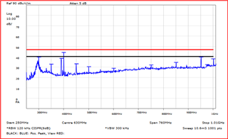
The emissions associated with this device is the broadband noise centered just below 300MHz. There is also a tone at 300MHz and other 50MHz harmonics which is independent (caused by a TI phy RMII ethernet interface ;() which we are investigating in parallel.
The TPS628510 is operating at 2MHz converting from 5V to 1.8V. Using a spectrum analyser to observe the noise on the 5V input rail I see this:
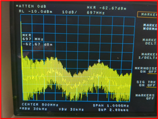
The 697MHz centred broadband noise is caused by ringing on the switch node. As an aside, I was able to reduce this level by 10dB by adding a snubber to control the ringing. But this is not the cause.
The broadband emission from DC-300MHz is caused by the TPS628510 (if I zoom in, I can see 2MHz comb lines matching the SMPS operating frequency). We believe the 300MHz broadband emission is being radiated by the 5V plane on the PCB. Using near-field probes we are clearly able to see this 300MHz broadband emission emanating from the area of the 5V plane.
We have various ideas on how to reduce emissions (e.g. moving from 4 to 6 layer PCB and enclosing 5V rail in fenced ground planes, and/or adding ferrite/capacitor filter at input to stop the noise getting back onto the 5V rail).
But before we move to re-spin the board, I wanted to enquire about the SSC option mentioned in the datasheet 9.3.3. How can it be enabled?
Thank you for helping!
Ben
