This thread has been locked.

If you have a related question, please click the "Ask a related question" button in the top right corner. The newly created question will be automatically linked to this question.

UCC28070: Abnormal waveform of AC input current

Part Number: UCC28070

Tool/software:

Hi 

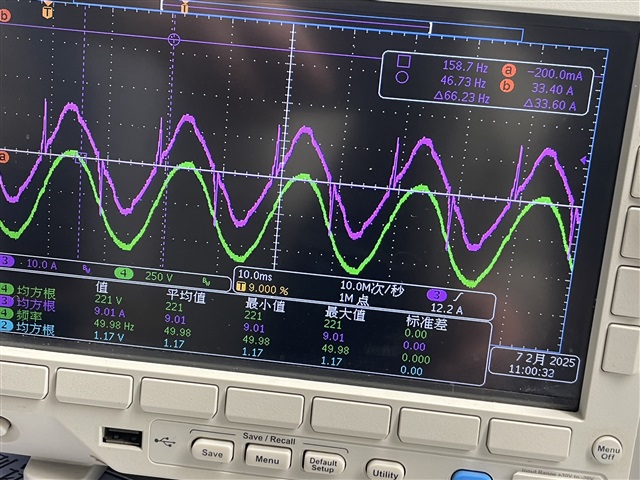
Test the AC current waveform at the input end, there is a peak at the purple zero point, and THD also exceeds the standard. Can it be optimized?

  • Hello User5883945,

    The current spike that occurs just after Vin increases above 0V at the zero-crossings is the result of excess duty cycle on GDA and GDB because CAOA and CAOB outputs are saturated at an internal 5V clamp.  At the zero-crossings, there is no voltage to develop current across the boost inductors, but the IMO output signal is driving the PWM to maximum to achieve some current.  Since there is no voltage, there is no current and the current error increases until the amplifiers' outputs saturate. 

    It takes a finite amount of time to desaturate the current-amp outputs and regain control over the duty cycle. During this desaturation time delay, PMW duty is maximum and as the input voltage does rise, so does the input current.  While the CAOx outputs are saturated, the inductor currents rise rapidly.  When CAOx finally gets out of saturation and reduces the  PWM duty down to control the current level, the current has formed a "spike" shape at the beginning of each half-cycle.  This does not happen at the end of each half-cycle because there the input voltage is falling instead of rising, so the current does not build up even as PWM duty goes to maximum. 

    There are two ways to eliminate these spikes:
    1.  Reduce the allowable DMAX by decreasing the value of Rdmx (R28 in your schematic).  Try reducing the value in small increments to see the progress of spike reduction.
    2.  Add a small offset voltage to each CSA and CSB input.  A resistor from CSA to VCC and from CSB to VCC can inject a little current into the Rcs resistors (R7 and R8 5.6R) to generate an offset voltage to make the CSx voltages appear higher than the IMO reference voltage at the zero-crossing.   
    I suggest starting with a low offset of ~15mV and increase the offset in small steps until the spikes disappear.  
    15mV/5.6R = ~2.7mA.  Since VCC = ~15V, 15V/2.7mA = 5600R.  I suggest to add a 4.7~5.6kR from each CSx input to VCC and evaluate the spike amplitude. 
    Add another resistor in parallel at each input to assess the progress of reducing the spike to zero.  

    You can implement both recommendations at the same time, if you wish.  A little bit of DMAX reduction plus a little bit of offset voltage. 
    Note: too much reduction of DMAX or too much offset voltage will eliminate the spikes, but also introduce excessive dead-time with zero-current at the zero-crossings. 
    Flat spots at the zero-crossing also increase current distortion.   
    So make small changes to optimize the spike reduction and obtain minimum THDi. 

    Regards,
    Ulrich