This thread has been locked.

If you have a related question, please click the "Ask a related question" button in the top right corner. The newly created question will be automatically linked to this question.

UCC14240-Q1: TUNING

Part Number: UCC14240-Q1
Other Parts Discussed in Thread: UCC14241-Q1,

Tool/software:

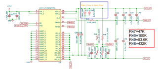
Hi, I'm designing a power supply for my gate driver.

The specifications for the gate driver are:

  • VCC: 15 V
  • VEE: 8 V

However, I am experiencing excessive ripple when using this configuration. I will share the schematic and waveform for further reference. The total gate charge (QG) is 1300 nC, and with 3 gates in parallel, the total is 3 * 1300 nC.

Could you help me fine-tune the values? The current limit resistor is 780 ohms. Also, could you provide a fault list for when the system turns off and how to properly turn it back on?


    1. Recommend to use UCC14241-Q1 or UCC15240/1-Q1 instead of UCC14240-Q1. UCC14240-Q1 was the first variant release. Some design improvements related to improved startup and better noise immunity are captured in all variants after UCC14240-Q1.
    2. P=Q*V*F=(3*1.3μC)*23V*20kHz=1.8W, assuming your gate driver frequency is 20kHz?
    3. Some of your capacitor values can be improved (COUT1b)...see attached Excel Design Sheet
    4. Suggest to RLIM set up as RDR configuration - see attached Excel
    5. List of faults are:
    • The powergood pin (/PG) output includes these fault monitor items:
      • UVPFBVDD = Under Voltage Protection FBVDD: (FBVDD < 2.25V which is 0.9 * VregVDD-VEE) = -10%
        • Latching SD fault that ust be reset by toggle EN or toggle VIN
      • OVPFBVDD = Over Voltage Protection FBVDD: (FBVDD > 2.75V which is 1.10 * VregVDD-VEE) = +10%
        • Latching SD fault that ust be reset by toggle EN or toggle VIN
      • UVPFBVEE = Under Voltage Protection FBVEE: (FBVEE < 2.25V which is 0.9 * VregCOM-VEE) = -10%
        • Latching SD fault that ust be reset by toggle EN or toggle VIN
      • UVPFBVEE = Over Voltage Protection FBVEE: (FBVEE > 2.75V which is 1.10 * VregCOM-VEE) = +10%
        • Latching SD fault that ust be reset by toggle EN or toggle VIN
      • OVLO(VDD-VEE) = Over Voltage Lockout (VDD-VEE):  (VDD-VEE) > 31V  absolute value at the pins.
        • Latching SD fault that ust be reset by toggle EN or toggle VIN
      • OVLOVIN = Over Voltage Lockout VIN:  (VIN-GNDP) > 31V  absolute value at the pins.
        • Non-latching SD, recovers when VIN is reduced to valid range
      • UVLOVIN = Under Voltage Lockout VIN:  (VIN-GNDP) < 20 V  absolute value at the pins.
        • Non-latching SD, recovers when VIN is increased to valid range
      • OTPprimary = Over Temperature Protection primary: Tj primary side > 150degC.
        • Non-latching SD, recovers when primary side die , over-temperature is reduced to valid range
      • OTPsecondary = Over Temperature Protection secondary: Tj secondary side > 150degC.
        • Non-latching SD, recovers when secondary side die, over-temperature is reduced to valid range

     UCC1424x-Q1_Calculator_V8_TI_02072025.xlsx

    Regards,

    Steve