Other Parts Discussed in Thread: MSPM0L1304, BQ79616,
Tool/software: CCS Theia (IDE), MSPM0L1304 (host MCU)
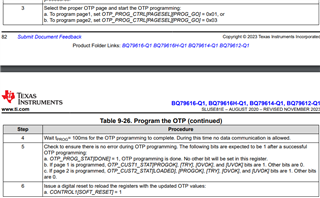
Here is my code (with some irrelevant portions deleted). On lines 187 and 247, it is detected that the OTP programming is locked. I checked to make sure that I was following the correct procedures in the BQ79616 datasheet, but I can't see anything I'm doing wrong. Please help!
/*
 * Copyright (c) 2023, Texas Instruments Incorporated
 * All rights reserved.
 *
 * Redistribution and use in source and binary forms, with or without
 * modification, are permitted provided that the following conditions
 * are met:
 *
 * *  Redistributions of source code must retain the above copyright
 *    notice, this list of conditions and the following disclaimer.
 *
 * *  Redistributions in binary form must reproduce the above copyright
 *    notice, this list of conditions and the following disclaimer in the
 *    documentation and/or other materials provided with the distribution.
 *
 * *  Neither the name of Texas Instruments Incorporated nor the names of
 *    its contributors may be used to endorse or promote products derived
 *    from this software without specific prior written permission.
 *
 * THIS SOFTWARE IS PROVIDED BY THE COPYRIGHT HOLDERS AND CONTRIBUTORS "AS IS"
 * AND ANY EXPRESS OR IMPLIED WARRANTIES, INCLUDING, BUT NOT LIMITED TO,
 * THE IMPLIED WARRANTIES OF MERCHANTABILITY AND FITNESS FOR A PARTICULAR
 * PURPOSE ARE DISCLAIMED. IN NO EVENT SHALL THE COPYRIGHT OWNER OR
 * CONTRIBUTORS BE LIABLE FOR ANY DIRECT, INDIRECT, INCIDENTAL, SPECIAL,
 * EXEMPLARY, OR CONSEQUENTIAL DAMAGES (INCLUDING, BUT NOT LIMITED TO,
 * PROCUREMENT OF SUBSTITUTE GOODS OR SERVICES; LOSS OF USE, DATA, OR PROFITS;
 * OR BUSINESS INTERRUPTION) HOWEVER CAUSED AND ON ANY THEORY OF LIABILITY,
 * WHETHER IN CONTRACT, STRICT LIABILITY, OR TORT (INCLUDING NEGLIGENCE OR
 * OTHERWISE) ARISING IN ANY WAY OUT OF THE USE OF THIS SOFTWARE,
 * EVEN IF ADVISED OF THE POSSIBILITY OF SUCH DAMAGE.
 */

#include "ti/devices/msp/m0p/mspm0l130x.h"
#include "ti/driverlib/dl_timerg.h"
#include "ti/driverlib/dl_uart_main.h"
#include "ti/driverlib/m0p/dl_interrupt.h"
#include "ti_msp_dl_config.h"
#include <math.h>
#include <stdint.h>

/* Configurations */
#define BQ79616_WAKE_PORT GPIOA
#define BQ79616_WAKE_PIN DL_GPIO_PIN_0
#define THERMISTOR_CONNECTION_R1 10 // kohms
#define THERMISTOR_T0 298.15 // Kelvins
#define THERMISTOR_R0 10 // kohms
#define THERMISTOR_B_25_85 3434 // Kelvins

/* BQ79616 addresses */
#define BQ79616_DEVICE_ADDR 0x00
#define OTP_ECC_TEST_ADDR 0x034C
#define CONTROL1_ADDR 0x0309
#define CONTROL2_ADDR 0x030A
#define DIR0_ADDR_ADDR 0x0306
#define COMM_CTRL_ADDR 0x0308
#define OTP_CUST1_STAT_ADDR 0x051A
#define OTP_CUST2_STAT_ADDR 0x051B
#define OTP_PROG_UNLOCK1A_ADDR 0x0300
#define OTP_PROG_UNLOCK2A_ADDR 0x0352
#define OTP_PROG_STAT_ADDR 0x0519
#define OTP_PROG_CTRL_ADDR 0x030B
#define DEV_CONF_ADDR 0x0002
#define ACTIVE_CELL_ADDR 0x0003
#define OV_THRESH_ADDR 0x0009
#define UV_DISABLE1_ADDR 0x000C
#define GPIO_CONF1_ADDR 0x000E
#define FAULT_MSK1_ADDR 0x0016
#define PWR_TRANSIT_CONF_ADDR 0x0018
#define ADC_CTRL1_ADDR 0x030D
#define VCELL16_HI_ADDR 0x0568
#define TSREF_HI_ADDR 0x058C
#define BAL_CTRL2_ADDR 0x032F
#define CB_CELL16_CTRL_ADDR 0x0318
#define FAULT_RST1_ADDR 0x0331
#define FAULT_SUMMARY_ADDR 0x052D
#define FAULT_SYS_ADDR 0x0536

/* BQ79616 Error Flags */
#define OTP_FAULT (1 << 0)
#define COMMS_FAULT (1 << 1)
#define POWER_RAIL_FAULT (1 << 2)
#define DIE_TEMP_FAULT (1 << 3)
#define LFO_FREQ_FAULT (1 << 4)

#define BUFFER_SIZE 512
#define MESSAGE_TYPE_NUM_BITS 3

/* Message Types */
#define REQ_INFO 0b000
#define VOLTAGE_THRESHOLD 0b001
#define TEMP_THRESHOLD 0b010
#define BALANCING 0b011
#define VOLTAGE 0b100
#define TEMP 0b101
#define ERROR 0b110
#define INIT 0b111
#define INIT_SUCCESS 0xFF

/* BQ79616 Request Types */
#define SINGLE_DEVICE_READ 0b000
#define SINGLE_DEVICE_WRITE 0b001
#define STACK_READ 0b010
#define STACK_WRITE 0b011
#define BROADCAST_READ 0b100
#define BROADCAST_WRITE 0b101
#define BROADCAST_WRITE_REVERSE 0b110

/* Global Variables */
uint16_t cell_voltages[17]; // measured in mV
volatile bool enable_balancing_req[17];
volatile bool stop_balancing_req[17];
int16_t temp1 = -10000; // measured in 0.01 degrees C
int16_t temp2 = -10000; // measured in 0.01 degrees C
volatile uint16_t ignore_voltage_threshold = 1000; // measured in mV
volatile int16_t ignore_temp_threshold = -2000; // measured in 0.01 degrees C
volatile bool awaiting_data = false;
volatile bool awaiting_faults = false;
volatile uint8_t module_num;
volatile uint8_t num_modules;
volatile uint8_t messages[BUFFER_SIZE];
uint16_t next_message_to_send_index = 0;
volatile uint16_t next_message_to_save_index = 0;
uint8_t bq79616_response_data[128];
volatile uint32_t micros = 0;

/* Function Prototypes */
void wake_bq79616(void);
void auto_address_bq79616(void);
bool program_bq79616_otp(void);
bool program_bq79616_otp_page1(void);
bool program_bq79616_otp_page2(void);
void set_bq79616_otp_settings(void);
void reset_bq79616_faults(void);
void bq79616_faults(void);
void command_bq79616(uint8_t req_type, uint8_t dev_addr, uint16_t reg_addr, uint8_t *data, uint8_t data_len);
uint8_t response_bq79616(void);
uint16_t crc_bq79616(const uint8_t *data, uint8_t length);
void delay_us(uint32_t us);
void micros_counter(void);

int main(void) {
    SYSCFG_DL_init();

    NVIC_EnableIRQ(MICROS_INST_INT_IRQN);
    DL_Interrupt_registerInterrupt(MICROS_INST_INT_IRQN, micros_counter);

    wake_bq79616();
    auto_address_bq79616();
    reset_bq79616_faults();
    program_bq79616_otp();
}

bool program_bq79616_otp(void) {
    if (program_bq79616_otp_page2() || program_bq79616_otp_page1()) {
        return true;
    } else { // neither OTP programming was successful - try one more time
        if (program_bq79616_otp_page2() || program_bq79616_otp_page1()) {
            return true;
        } else { // error - neither OTP programming was successful
            return false;
        }
    }
}

bool program_bq79616_otp_page1(void) {
    uint8_t data[4];

    data[0] = 0b000;
    command_bq79616(SINGLE_DEVICE_READ, BQ79616_DEVICE_ADDR, OTP_CUST1_STAT_ADDR, data, 1);
    if (response_bq79616() == 0) {
        return false;
    }
    if ((bq79616_response_data[0] & 1) == 0) { // page 1 not yet programmed
        // Unlock the OTP programming
        data[0] = 0x02;
        data[1] = 0xB7;
        data[2] = 0x78;
        data[3] = 0xBC;
        command_bq79616(SINGLE_DEVICE_WRITE, BQ79616_DEVICE_ADDR, OTP_PROG_UNLOCK1A_ADDR, data, 4);

        // Check to confirm the OTP unlock procedure is successful
        data[0] = 0b000;
        command_bq79616(SINGLE_DEVICE_READ, BQ79616_DEVICE_ADDR, OTP_PROG_STAT_ADDR, data, 1);
        if (response_bq79616() == 0) {
            return false;
        }
        if ((bq79616_response_data[0] >> 7) != 1) { // error - OTP programming locked
            return false;
        }

        // Select the proper OTP page and start the OTP programming
        data[0] = 0x01;
        command_bq79616(SINGLE_DEVICE_WRITE, BQ79616_DEVICE_ADDR, OTP_PROG_CTRL_ADDR, data, 1);

        // Do the OTP programming
        set_bq79616_otp_settings();

        // Wait 100 ms for the OTP programming to complete.
        delay_us(100000);

        // Check to ensure there is no error during OTP programming.
        data[0] = 0b000;
        command_bq79616(SINGLE_DEVICE_READ, BQ79616_DEVICE_ADDR, OTP_PROG_STAT_ADDR, data, 1);
        if (response_bq79616() == 0) {
            return false;
        }
        if ((bq79616_response_data[0] & 1) != 1) { // error - unsuccessful OTP programming
            return false;
        }
        command_bq79616(SINGLE_DEVICE_READ, BQ79616_DEVICE_ADDR, OTP_CUST1_STAT_ADDR, data, 1);
        if (response_bq79616() == 0) {
            return false;
        }
        if (bq79616_response_data[0] != 0b00001111) { // error - unsuccessful OTP programming
            return false;
        }

        // Issue a digital reset to reload the registers with the updated OTP values
        data[0] = 0b10;
        command_bq79616(SINGLE_DEVICE_WRITE, BQ79616_DEVICE_ADDR, CONTROL1_ADDR, data, 1);
    }
    return true;
}

bool program_bq79616_otp_page2(void) {
    uint8_t data[4];

    data[0] = 0b000;
    command_bq79616(SINGLE_DEVICE_READ, BQ79616_DEVICE_ADDR, OTP_CUST2_STAT_ADDR, data, 1);
    if (response_bq79616() == 0) {
        return false;
    }
    if ((bq79616_response_data[0] & 1) == 0) { // page 2 not yet programmed
        // Unlock the OTP programming
        data[0] = 0x7E;
        data[1] = 0x12;
        data[2] = 0x08;
        data[3] = 0x6F;
        command_bq79616(SINGLE_DEVICE_WRITE, BQ79616_DEVICE_ADDR, OTP_PROG_UNLOCK2A_ADDR, data, 4);

        // Check to confirm the OTP unlock procedure is successful
        data[0] = 0b000;
        command_bq79616(SINGLE_DEVICE_READ, BQ79616_DEVICE_ADDR, OTP_PROG_STAT_ADDR, data, 1);
        if (response_bq79616() == 0) {
            return false;
        }
        if ((bq79616_response_data[0] >> 7) != 1) { // error - OTP programming locked
            return false;
        }

        // Select the proper OTP page and start the OTP programming
        data[0] = 0x03;
        command_bq79616(SINGLE_DEVICE_WRITE, BQ79616_DEVICE_ADDR, OTP_PROG_CTRL_ADDR, data, 1);

        // Do the OTP programming
        set_bq79616_otp_settings();

        // Wait 100 ms for the OTP programming to complete.
        delay_us(100000);

        // Check to ensure there is no error during OTP programming.
        data[0] = 0b000;
        command_bq79616(SINGLE_DEVICE_READ, BQ79616_DEVICE_ADDR, OTP_PROG_STAT_ADDR, data, 1);
        if (response_bq79616() == 0) {
            return false;
        }
        if ((bq79616_response_data[0] & 1) != 1) { // error - unsuccessful OTP programming
            return false;
        }
        command_bq79616(SINGLE_DEVICE_READ, BQ79616_DEVICE_ADDR, OTP_CUST2_STAT_ADDR, data, 1);
        if (response_bq79616() == 0) {
            return false;
        }
        if (bq79616_response_data[0] != 0b10001111) { // error - unsuccessful OTP programming
            return false;
        }

        // Issue a digital reset to reload the registers with the updated OTP values
        data[0] = 0b10;
        command_bq79616(SINGLE_DEVICE_WRITE, BQ79616_DEVICE_ADDR, CONTROL1_ADDR, data, 1);
    }
    return true;
}

void set_bq79616_otp_settings(void) {
    uint8_t data[2];

    data[0] = 0b1100000;
    command_bq79616(SINGLE_DEVICE_WRITE, BQ79616_DEVICE_ADDR, DEV_CONF_ADDR, data, 1);

    data[0] = 0xA;
    command_bq79616(SINGLE_DEVICE_WRITE, BQ79616_DEVICE_ADDR, ACTIVE_CELL_ADDR, data, 1);

    data[0] = 0x2E;
    command_bq79616(SINGLE_DEVICE_WRITE, BQ79616_DEVICE_ADDR, OV_THRESH_ADDR, data, 1);

    data[0] = 0xFF;
    data[1] = 0xFF;
    command_bq79616(SINGLE_DEVICE_WRITE, BQ79616_DEVICE_ADDR, UV_DISABLE1_ADDR, data, 2);

    data[0] = 0b00010010;
    command_bq79616(SINGLE_DEVICE_WRITE, BQ79616_DEVICE_ADDR, GPIO_CONF1_ADDR, data, 1);

    data[0] = 0b11111100;
    data[1] = 0b0011110;
    command_bq79616(SINGLE_DEVICE_WRITE, BQ79616_DEVICE_ADDR, FAULT_MSK1_ADDR, data, 2);

    data[0] = 0b00000;
    command_bq79616(SINGLE_DEVICE_WRITE, BQ79616_DEVICE_ADDR, PWR_TRANSIT_CONF_ADDR, data, 1);
}

void reset_bq79616_faults(void) {
    uint8_t data[2];

    data[0] = 0xFF;
    data[1] = 0xFF;
    command_bq79616(SINGLE_DEVICE_WRITE, BQ79616_DEVICE_ADDR, FAULT_RST1_ADDR, data, 2);

    data[0] = 0x00;
    data[1] = 0x00;
    command_bq79616(SINGLE_DEVICE_WRITE, BQ79616_DEVICE_ADDR, FAULT_RST1_ADDR, data, 2);
}

void wake_bq79616(void) {
    // Disable UART to allow pin mode changes
    DL_UART_Main_disable(BQ79616_INST);

    // Configure pin as GPIO output
    DL_GPIO_initDigitalOutput(GPIO_BQ79616_IOMUX_TX);
    DL_GPIO_enableOutput(BQ79616_WAKE_PORT, BQ79616_WAKE_PIN);

    // Drive low for 2-2.5 ms
    DL_GPIO_clearPins(BQ79616_WAKE_PORT, BQ79616_WAKE_PIN);
    delay_us(2300);

    // Drive high again
    DL_GPIO_setPins(BQ79616_WAKE_PORT, BQ79616_WAKE_PIN);

    // Wait 10 + 0.6 * number of devices ms before any further comms
    delay_us(10600);

    // Reconfigure the pin back to UART TX function
    DL_GPIO_initPeripheralOutputFunction(
        GPIO_BQ79616_IOMUX_TX, GPIO_BQ79616_IOMUX_TX_FUNC
    );

    // Re-enable UART
    DL_UART_Main_enable(BQ79616_INST);
}

void auto_address_bq79616(void) {
    uint8_t data[1];
    uint8_t num_tries = 0;

    while (num_tries++ < 3) {
        // Dummy broadcast write OTP_ECC_TEST=0x00 to sync the DLL (delay-locked loop)
        data[0] = 0x00;
        command_bq79616(BROADCAST_WRITE, 0, OTP_ECC_TEST_ADDR, data, 1);

        // Enable auto addressing mode by broadcast writing CONTROL1=0x01
        data[0] = 0x01;
        command_bq79616(BROADCAST_WRITE, 0, CONTROL1_ADDR, data, 1);

        // Loop through the total number of boards setting the DIR0_ADDR of each board
        data[0] = BQ79616_DEVICE_ADDR;
        command_bq79616(BROADCAST_WRITE, 0, DIR0_ADDR_ADDR, data, 1);

        // Broadcast write everything as a stack device first (COMM_CTRL=0x02)
        data[0] = 0x02;
        command_bq79616(BROADCAST_WRITE, 0, COMM_CTRL_ADDR, data, 1);

        // Set device as base and top of stack (COMM_CTRL=0x01)
        data[0] = 0x01;
        command_bq79616(SINGLE_DEVICE_WRITE, BQ79616_DEVICE_ADDR, COMM_CTRL_ADDR, data, 1);

        // Dummy broadcast read OTP_ECC_TEST to sync the DLL
        data[0] = 0b000;
        command_bq79616(BROADCAST_READ, 0, OTP_ECC_TEST_ADDR, data, 1);
        if (response_bq79616() == 0) {
            continue; // try again
        }

        break;
    }
}

void command_bq79616(uint8_t req_type, uint8_t dev_addr, uint16_t reg_addr, uint8_t *data, uint8_t data_len) {
    uint8_t frame[14];
    uint8_t frame_len = 0;

    frame[frame_len++] = ((1 << 7) | (req_type << 4)) | (data_len - 1);

    if (req_type == SINGLE_DEVICE_READ || req_type == SINGLE_DEVICE_WRITE) {
        frame[frame_len++] = dev_addr;
    }

    frame[frame_len++] = (uint8_t)(reg_addr >> 8);
    frame[frame_len++] = (uint8_t)(reg_addr & 0xFF);

    for (uint8_t i = 0; i < data_len; i++) {
        frame[frame_len++] = data[i];
    }

    uint16_t crc = crc_bq79616(frame, frame_len);
    frame[frame_len++] = (uint8_t)(crc >> 8);
    frame[frame_len++] = (uint8_t)(crc & 0xFF);

    for (uint8_t i = 0; i < frame_len; i++) {
        DL_UART_Main_transmitDataBlocking(BQ79616_INST, frame[i]);
    }
}

// returns 0 on CRC error - try again if required
uint8_t response_bq79616(void) {
    uint8_t init_byte = DL_UART_Main_receiveDataBlocking(BQ79616_INST);
    uint8_t data_len = init_byte + 1;

    uint8_t frame[6 + data_len];
    uint8_t frame_len = 0;

    frame[frame_len++] = init_byte;

    frame[frame_len++] = DL_UART_Main_receiveDataBlocking(BQ79616_INST); // device address byte

    frame[frame_len++] = DL_UART_Main_receiveDataBlocking(BQ79616_INST); // register address byte 1
    frame[frame_len++] = DL_UART_Main_receiveDataBlocking(BQ79616_INST); // register address byte 2

    for (uint8_t i = 0; i < data_len; i++) {
        bq79616_response_data[i] = DL_UART_Main_receiveDataBlocking(BQ79616_INST);
        frame[frame_len++] = bq79616_response_data[i];
    }

    frame[frame_len++] = DL_UART_Main_receiveDataBlocking(BQ79616_INST); // CRC byte 1
    frame[frame_len++] = DL_UART_Main_receiveDataBlocking(BQ79616_INST); // CRC byte 2

    if (crc_bq79616(frame, frame_len) != 0x0000) { // error - CRC wrong
        // clear RX FIFO
        while (!DL_UART_Main_isRXFIFOEmpty(BQ79616_INST)) {
            DL_UART_Main_receiveData(BQ79616_INST);
        }
        return 0;
    }

    return data_len;
}

uint16_t crc_bq79616(const uint8_t *data, uint8_t length) {
    uint16_t crc = 0xFFFF;
    for (uint8_t i = 0; i < length; i++) {
        uint8_t byte = data[i];
        // Process each bit of the byte
        for (uint8_t bit = 0; bit < 8; bit++) {
            // XOR the LSB of CRC with the LSB of the data bit
            uint8_t lsb_crc = crc & 0x0001;
            uint8_t lsb_data = byte & 0x01;
            uint8_t xor_val = (lsb_crc ^ lsb_data);

            // Shift CRC right by 1
            crc >>= 1;

            // If XOR result is 1, XOR with polynomial
            if (xor_val) {
                crc ^= 0xA001; // Polynomial in LSB-first form
            }

            // Move to the next bit of the byte
            byte >>= 1;
        }
    }
    return (crc >> 8) | (crc << 8);
}

void delay_us(uint32_t us) {
    DL_TimerG_startCounter(MICROS_INST);
    uint32_t start = micros;
    while (micros - start < us) {}
    DL_TimerG_stopCounter(MICROS_INST);
}

/* Should not be called by our own program -- should only be called by the interrupt */
void micros_counter(void) {
    micros++;
}