This thread has been locked.

If you have a related question, please click the "Ask a related question" button in the top right corner. The newly created question will be automatically linked to this question.

TPS562242: Bad step response in my design

Part Number: TPS562242

Tool/software:

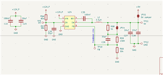
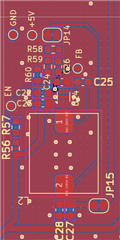
I designed some buck converters for my pcb, trying to follow the design guidelines specified in the datasheet and the values suggested. When testing the response to a transient consumption and ripple current I get pretty high values. What could cause this issue? Is it mainly a layout issue or more related to component selection?

  • Dear Sir,

    Pls kindly let me check your question and get back to you during these days. Thank you!

    BRs

    Lucia

  • Dear Ivan,

    Could you pls kindly share me the schematic? And what's the working condition?

    Thank you!

    BRs

    Lucia

  • Yes of course! I followed the component values recommended in the datasheet. When routing, I tried to follow the basic sketch provided in the datasheet and the design guidelines. Voltage wise it was accurate, but the transient response and noise is horrible. Thanks in advance for the help!


  • What do you mean with working condition?

  • Hi Ivan,

    For working condition, I am saying what's the VIN, VOUT and IOUT?

    BRs

    Lucia

  • Sorry for the misunderstanding. The operating conditions are:
    Vin: 12V
    Vout: 5V
    Iout: 0.5A Nominal / 1.2A Peak

  • Hi Ivan,

    Thanks for your feedback. Pls kindly let me check your schematic and get back to you during these days. 

    BRs

    Lucia

  • Hi Ivan,

    The schematic is good. For the layout, pls kindly find below comments:

    Keep VIN and GND traces as wide as possible to reduce trace impedance. The wide areas are also an advantage from the view point of heat dissipation.

    Place the input capacitor and output capacitor as close to the device as possible to minimize trace impedance.

    Make the trace of the FB node as small as possible to avoid noise coupling.

    You can find an example of the layout in datasheet 8.4.1.

    Thank you!

    BRs

    Lucia

  • Figure 8-16 from section 8.4.2 is pretty vague in terms of example layouts. I tried following figure 8-16 as shown in the attached picture from the previous reply. I was wondering if a cheap Output capacitor might be to blame for the bad step response? That is my only concern, as output ripple is tolerable, although high. Can it also be the inductor to blame?

    Thanks in advance for your time and help

  • Hi Ivan,

    Pls kindly let me check and get back to you during these days. Thank you!

    BRs

    Lucia

  • Have you had cases where the regulator stop working and shorts the input rail? I've had it happen two times now, and the cause is unknown. Can the regulator cause damage to itself with an unstable output response, is it possible or is it protected against an unstable output?.

  • Hi Ivan,

    Do you mean that the device will be damaged and the VIN pin short to GND pin?

    Thank you!

    BRs

    Lucia

  • Yes, the device shorts VIN to GND. Can the regulator do that because of an unstable output response or is it exclusively a input condition that the regulator can fail in such a way?

  • Hi Ivan,

    In general, it will not be related with the unstable output, but I would recommend you can check below ways if there is VIN to GND short.

    Vin Cap too far away causing SW spike too high or too negative to cause LSF or HSF damage

    Input voltage surge/ESD

    Input power supply bad performance

    Inductor saturation current too small

    Peripheral components missing/quality issue (Vin Cap, Boot Cap, FB resistor, etc.) causing internal logic mal-function

    IC pin to pin short causing EOS

    Soldering quality issue causes components open/short or IC pin open or pin to pin short

    Thank you!

    BRs

    Lucia

  • Thanks. I think it is a bad input power supply that has a negative transient. Even though I have a reverse blocking diode in series. I think it is not fast enough.

    Regarding output instability mentioned earlier. Can a cheap capacitor with high ESR or highly derated at high frequencies be the cause of the instability? I am leaning to that being the cause, but i am not certain that it could cause those kinds of output responses.

  • Dear Ivan,

    I would recommend you can follow the datasheet LC table. In general, when we design our devices, we simulate a couple of LC combinations and also validate a couple of those combinations in our labs and those combinations are then recommended in the datasheet. In general, when we design our devices, we simulate a couple of LC combinations and also validate a couple of those combinations in our labs and those combinations are then recommended in the datasheet.

    Refer below app for stability check:

    Simplifying Stability Checks (Rev. B)

    Refer below app for DCAP stability design:

    Stability Analysis and Design of D-CAP2 and D-CAP3 Converter – Part 1

    Thank you!

    BRs

    Lucia

  •   Thanks for the reply. As previously stated, I tried following everything the datasheet said. Component Values, inductor ratings, layout guidelines and recommendations, etc. I have a small lab and cannot measure very much, that is why I asked for help here. Simplifying stability checks is not really helpfull, as i know my system is unstable. Stability Analysis and Design of D-CAP2 and D-CAP3 is a very generic document outlying the general transfer function of converters with D-CAP control mode, it does not help very much as it does not provide values for most of the transfer function.

    Best regards, Ivan.