This thread has been locked.

If you have a related question, please click the "Ask a related question" button in the top right corner. The newly created question will be automatically linked to this question.

TPS55288: Vin limitation at 100W , Vout=20V, Iout=5A

Part Number: TPS55288
Other Parts Discussed in Thread: , PMP40801

Tool/software:

Hi, 

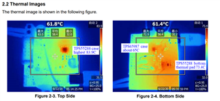
according to the TPS55288EVM-045 Evaluation Module (slvubo4b) the input voltage must be 12V or higher if 100W (20V/5A) is going to be tested at output.

Could you tell us which component is bottleneck for Vin operation below 12V?

Webench allows simulation with these parameters, therefore I am asking why the Vin must be higher than 12V in the eval board.
Also, Webench doesn't allow simulation with Vout higher than 20V .Is this correct or I am doing something wrong in simulation?
Datasheet says Voutmax=22V and moreover there is a feature cable voltage drop compensation that can go +0,75V above target voltage, if I've understood that correctly.       


Could you please compare results between Webench and excel calculation sheet for the IC Pd parameter when it works in boost mode, Vin is the lowest? 
Should they match? 


BR

Josko

  • Hi Josko,

    Thank you for reaching out.

    12V is a recommended operating range for EVM board, not a must. You can operate the EVM board with Vin<12V. Notice that typical average inductor current limit is 16A. So with 100W output, minimum input voltage that can support output is 100/0.95/16=6.57V. Also, thermal performance should be considered. You may need to reduce the switching frequency for better thermal performance.

    Webench simulation is for reference. Your understanding is right, Device can output 22V with CDC function. Notice that device has minimum 22.5V OVP protection. Also, there is some overshoot voltage during load transient. So user should consideration VOUT OVP when setting the maximum output voltage.

    WEBENCH and excel tool result may not totally match. You can send me the schematic along with working spec and output cap part number after you finish the design. I can help check if the compensation parameters are suitable.

    Regards,

    Mulin

  • Hi Mulin, 

    thank you for quick response and your offer for the schematic and design review. 

    If it is ok for you, I would like to continue conversation here with questions related to the TPS55288 during schematic build up. Since I am checking TPS55288 documentation for the first time, some questions or remarks have been aroused.    

    1. 12V is a recommended operating range for EVM board, not a must. You can operate the EVM board with Vin<12V. Notice that typical average inductor current limit is 16A. So with 100W output, minimum input voltage that can support output is 100/0.95/16=6.57V. 

      1. Just to avoid confusion, Vin=6.57V is the typical minimum value for the Ta=+25°C. For the whole Tj operating temperature range -40°C~+150°C it will be 14A in the wors case, thus 100/0.95/14 = 7.52V, right? 
      2. What is the root of cause for higher current tolerances in the whole temperature range, external resistor connected at the ILIM(pin 17), or the IC itself?
      3. If it is about IC itself, then it doesn’t make sense to use Rsens resistor better than 20k 1% 100ppm/°C, right?

    2. "Also, thermal performance should be considered. You may need to reduce the switching frequency for better thermal performance.”

      1. Would it be possible to find out, whether thermal test were performed with eval boards or reference designs at +25°C only?
      2.  Could you please find out, which operating conditions (Vin, Vout, Iout, Tamb) were applied, as thermal images (Figure 2-3, and Figure 2-4) form the  document Test Report: PMP40801 were taken? 


      3.  Could you also please find out, which board was used for efficiency vs output current measeurements, Figure 6-10 from datasheet? 
        According to that  graph the last point for the efficiency @ 20V_out, 12V_vin, Ta=25°C was at 6A, right? 


      4. The main concern here is, whether the TPS55288 is the right choice for this application or we should go for something else, where all four MOSFETS are externally added. 

    3. For me personally it is confusing alittle bit to see binary format with the "h" notification at end in the registers description.
      For example: 
      IOUT_LIMIT Register (Address = 2h) [reset = 11100100h]
      Wouldn't be better to have either:   
      IOUT_LIMIT Register (Address = 2h) [reset = E4h
      or
      IOUT_LIMIT Register (Address = 2h) [reset = 11100100b
    4. In the Table 7-5. IOUT_LIMIT Register Field Descriptions look like only few current limit targets are supported. 
      I would prefer description in this format: 

      Sets the current limit target voltage between the ISP pin and the ISN

      Pin (in 0,5mV steps)

      0000000b = VISP-VISN = 0 (mV)

      0000001b = VISP-VISN = 0.5 (mV)

      0000010b = VISP-VISN = 1 (mV)

      0000011b = VISP-VISN = 1.5 (mV)

      0000100b = VISP-VISN = 2.0 (mV)

      ….

      1100100b = VISP-VISN = 50.0 (mV) (Default)

      ….

      1111111b = VISP-VISN = 63.5 (mV)


    5. Is there any particular reason, why reference designs and eval boards use 102k at some locations instead 100k?
      For example: Schematic — PMP40801 R11.    


    Can I message you our target requirements for design?  

    BR
    Josko

  • Hi Josko,

    I agree that the first thing we discuss is that if TPS55288 is suitable for your design. So can you help provide below information:

    1.What is the application here?

    2.What is the minimum input voltage in your design?

    3.What is the board size in your design? What is the copper thickness?

    4.What is the temp rise requirement in your design? What is the maximum ambient temperature?

    You can send me friendship request if it cannot be discussed in public.

    About your questions:

    Just to avoid confusion, Vin=6.57V is the typical minimum value for the Ta=+25°C. For the whole Tj operating temperature range -40°C~+150°C it will be 14A in the wors case, thus 100/0.95/14 = 7.52V, right? 

    yes.

    • What is the root of cause for higher current tolerances in the whole temperature range, external resistor connected at the ILIM(pin 17), or the IC itself?
    • If it is about IC itself, then it doesn’t make sense to use Rsens resistor better than 20k 1% 100ppm/°C, right?

    Main root cause is IC itself. The RLIM resistor is also important. 1% accuracy is good enough.

    • Would it be possible to find out, whether thermal test were performed with eval boards or reference designs at +25°C only?
    •  Could you please find out, which operating conditions (Vin, Vout, Iout, Tamb) were applied, as thermal images (Figure 2-3, and Figure 2-4) form the  document Test Report: PMP40801 were taken? 

    I don't have this information. I can provide EVM thermal performance. Do you have NDA with TI?

     Could you also please find out, which board was used for efficiency vs output current measeurements, Figure 6-10 from datasheet? 
    According to that  graph the last point for the efficiency @ 20V_out, 12V_vin, Ta=25°C was at 6A, right? 

    Efficiency is test in EVM board.

    the 6A curve is 9V Vin. For 12V Vin, maximum output current is 8A.

    The main concern here is, whether the TPS55288 is the right choice for this application or we should go for something else, where all four MOSFETS are externally added. 

    Yes, so let's discuss about the working spec as above.

    About point 3 and 4, thank you for your advice, we will consider it in next version

    Is there any particular reason, why reference designs and eval boards use 102k at some locations instead 100k?

    102k with 11.3k resistor get 12V output. There is no special requirement for the value. 100k is also ok.

    Regards,

    Mulin

  • Hi Mulin, 

    I've just sent your friendship request. 

    I don't have this information. I can provide EVM thermal performance. Do you have NDA with TI?

    Yes, we have NDA signed. I wrote to TI's FAE which is in charge for us, to get in touch with you and confirm this information or forward you the NDA. 


    BR

    Josko

  • Hi Josko,

    I have received NDA confirmation. I sent you the EVM thermal performance. Please send me the working condition as I asked above.

    Regards,

    Mulin