A related question is a question created from another question. When the related question is created, it will be automatically linked to the original question.
If you have a related question, please click the "Ask a related question" button in the top right corner. The newly created question will be automatically linked to this question.
1)I have two output configurations: 5V/8A(for 9-36Vin) and 8V/8A(for 12-36Vin), please see attached files. From the two settings, I can use 3.3uH inductor for both 5V and 8V output, am I right?
2) for compensation components, I use same RC1/CC1/CC2 for 8V out as 5V output, that's OK?
Is it possible to change from 5V fixed output to 5V adjustable output where feedback resistors are used? The efficiency will get a small gain bump by using feedback resistors. This is due to the VCC drive to the internal FETs. Fixed output options of 3.3V and 5V have a gate drive of 5V whereas adjustable output configuration has a gate drive of 8V.
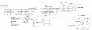
The inductor needs to have a higher Isat rating for this application. If we sent the current limit to 9A, the recommended sense resistance is 5.5ohms. Currently, the sense resistor chosen is 5mohms which is the minimum amount that the part can use based on the Recommended Operating Conditions found in the datasheet. The calculator calculates that the Minimum Inductor Sat Current needs to be 12.4A, which is higher than what is shown in the schematic (11A).
Yes, you can use 3.3uH for this design.
The output capacitance on the schematic shows 8*22uF. The total capacitance with a voltage derating at 5V for a typical 22uF/25V/1210 capacitor is 80% of the intrinsic capacitance of the capacitor. Therefore, the derated amount on the output capacitance is around 141uF. This amount of output capacitance can support an output load step of 80% of the full-load output current (8A) that meets a 2% output voltage ripple spec. Please see quickstart calculator.
For the input voltage ripple the derated amount of capacitance placed on VIN was calculated to be 39.53uF. That amount of capacitance can support an input voltage ripple spec of around 140mV. Please see quickstart calculator.
The loop compensation was fine tuned based on the derated output capacitance value. Please see quickstart calculator.
Since VOUT is 5V, connecting the BIAS pin to VOUT will yield a slight performance improvement in efficiency. Please add a 1uF capacitor as close as possible to the BIAS pin for noise improvement. Please see quickstart calculator.
I was able to set the compensation to match both applications.
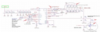
The inductor needs to have a higher Isat rating for this application. If we sent the current limit to 9A, the recommended sense resistance is 5.6ohms. Currently, the sense resistor chosen is 5mohms which is the minimum amount that the part can use based on the Recommended Operating Conditions found in the datasheet. The calculator calculates that the Minimum Inductor Sat Current needs to be 12.4A, which is higher than what is shown in the schematic (11A).
Yes, you can use 3.3uH for this design.
The output capacitance on the schematic shows 4*22uF for an 8V output. The total capacitance with a voltage derating at 8V for a typical 22uF/25V/1210 capacitor is 56.6% of the intrinsic capacitance of the capacitor. Therefore, the derated amount on the output capacitance is around 49.8uF. This amount of output capacitance will not support an output load step of 80% of the full-load output current (8A) that meets a 2% output voltage ripple spec. I suggest adding one more 22uF capacitor, a total of 5*22uF to the design. This will bring the total derated capacitance amount to 62.3uF and will meet the 2% output voltage ripple spec with an 80% load step. Please see quickstart calculator.
For the input voltage ripple the derated amount of capacitance placed on VIN was calculated to be 39.53uF. That amount of capacitance can support an input voltage ripple spec of around 140mV. Please see quickstart calculator.
The loop compensation was fine tuned based on the additional 22uF capacitor (total of 5*22uF) with the derated output capacitance value. Please see quickstart calculator.
Since VOUT is 8V, connecting the BIAS pin to VOUT will yield a slight performance improvement in efficiency. Please add a 1uF capacitor as close as possible to the BIAS pin for noise improvement. Please see quickstart calculator.
I was able to set the compensation to match both applications.