This thread has been locked.

If you have a related question, please click the "Ask a related question" button in the top right corner. The newly created question will be automatically linked to this question.

UCC28600: Follow-up:Issue with Flyback Converter Simulation in TINA-TI

Part Number: UCC28600
Other Parts Discussed in Thread: LM5023

Tool/software:

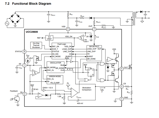
Thank you for the useful article from previous thread, SLUAAC5, that you shared! It provided great insights into the fault detection mechanisms, and I tried probing the CS and OVP pins as suggested. After making some updates to the schematic, based on reviewing the datasheet, I found that there is no longer an issue with the OVP pins.

However, I'm still facing some challenges with the Rcs and Rpl values. There seem to be multiple formulas for calculating them in the datasheet, and the design calculator uses a different approach. Could you kindly guide me on which method is more accurate or how to approach these calculations more effectively?

I’ve also attached waveforms for different input voltages. The converter now behaves as expected at both 120 VDC and 180 VDC inputs, but the primary current shape still doesn't appear as a smooth ramp. At a 250 VDC input, the output doesn't go above 5 volts, even though the primary current continues to increase when it should decrease. At 325 VDC, as shown in the attached waveform, it seems the OVP is not triggering, which could be related to the problem.

Could you provide further suggestions on resolving this issue? Also, if possible, could you recommend a flyback controllers that includes Output OVP functionality and can operate above 200kHz?

also I want to mention that the LM5023 was mentioned in previous post because the SPICE models I used are proven to be reliable, so I don’t think the issue is model-related.

Updated Schematic:https://workdrive.zohopublic.in/file/m492ucd8cc3e83a364cc6b0a90e9bdbc400df

Waveform at 120VDC input:https://workdrive.zohopublic.in/file/m492u5ff8c6947f4b4f50a412d70b7a5273d0

Waveform at 180VDC input:https://workdrive.zohopublic.in/file/m492uaa947a8f9e7844bfb0349eaa147a3f61

Waveform at 250VDC input:https://workdrive.zohopublic.in/file/m492u9774f21ad54041df8cc8c9ecc745ec0a

Waveform at 325VDC input:https://workdrive.zohopublic.in/file/m492uf86440051c0840ed9f9f13935836fcb3

Looking forward to your suggestions!

Regards,

  • Also AM3(in waveforms) is current sourced from OVP pin which is less than 450uA in all cases to trigger any OVP also I included soft start voltage as VSS and couldn't get you on soft start issue can you provide something for soft start 

  • Hello,


    Your inquiry has been received and is under review.


    Regards,

  • Hello,

    I looked at some of your waveforms and the primary current and it looks triangular.  That is what it should look like for zero current switching for QR flyback.  This should be controlled by V = Lpm*di/dt, di = Vcs/Rcs controlled.

    I did notice that you had some ringing on the currents after FET turnoff.  You might be able to resolve those issues with RC snubbers.


    The RPL resistor is used to try to remove current overshoot caused by delays in the controller and the system.  This  more of an issue for high line/max bulk voltage in your design.


    When the FET is on ILINE = Vin*Na/Np*Rovp1. ILINE/2 will go through the RPL when the FET is on and will move with changes in line voltage.

    What you want to do is set this resistance at maximum input voltage to turn off your FET early to remove current over shoot due to delays in the IC.  This will help with power limiting over the line.


    I would actually start with 100 ohms for RPL.  Bring the design up with 10% load to high line and slowly bring the design up to max load.  Then monitor the VCS pin and see where it is controlled to.  More than likely this will be more than VCS(max) due to the delays in the IC.

    I would then set RPL as follows:

    RPL = (VCS Measured – VCS(max))/(ILINE/2).  I believe for this design your VCS(max) should be around 1 V.  IN this way the design will not go into power limiting until 120% of the output power is reached.

    What this will due at high line is turn off the FET earlier so you have better controlled peak current throughout your design.


    If you are still having issues with the input current and need to dig deeper into that please repost in the e2e.


    Regards,