Other Parts Discussed in Thread: TPS55288EVM-045
Tool/software:
Hello,
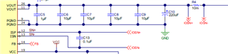
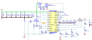
I am experiencing an issue while using the TPS552882RPMR. The VSYS is powered with 24V from a 10A bench power supply, and the output is configured for 12V/5A. However, the output current is limiting at 3.8A. Below is the detailed circuit design:
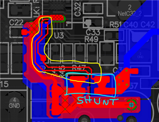
Additionally, here is the PCB layout showing the routing of the shunt resistor:
Tests Conducted So Far:
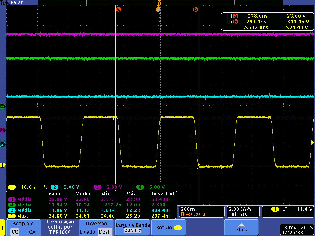
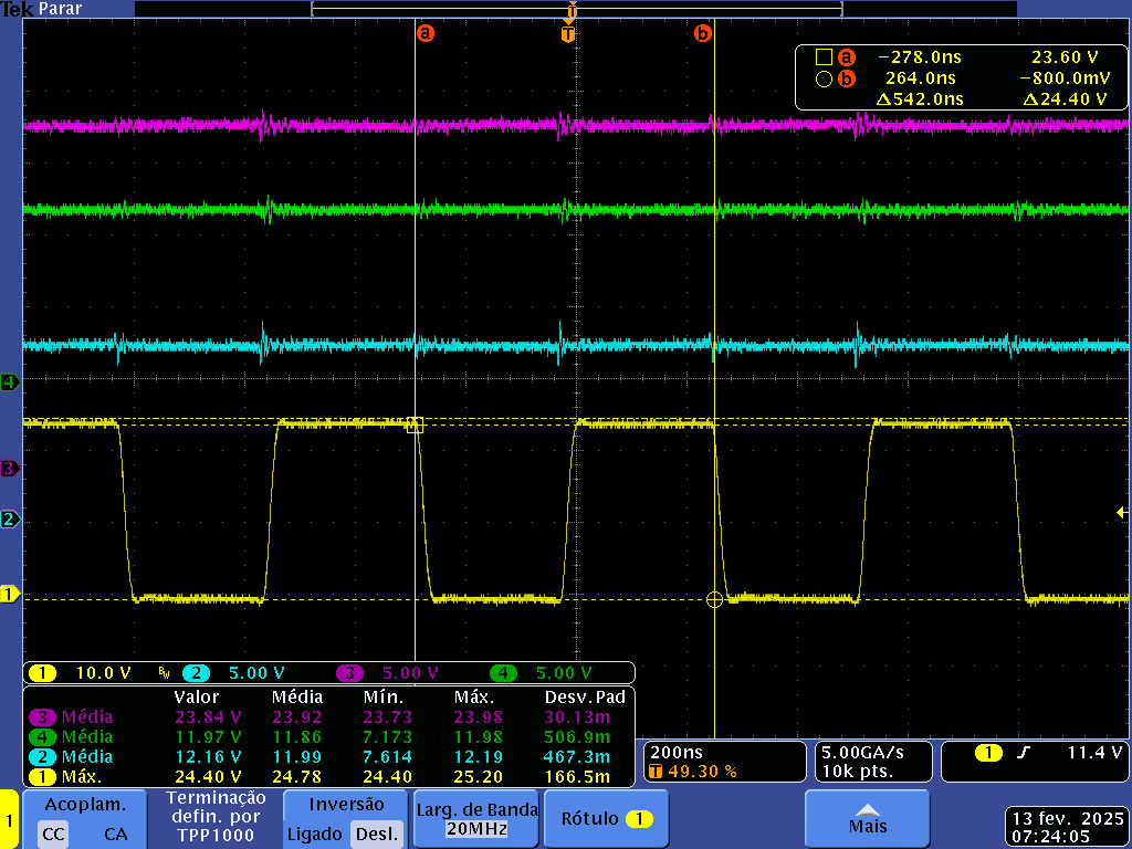
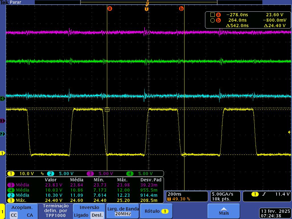
- I added a 100nF capacitor near the ISN and ISP pins, but the issue persists.
- I shorted ISN and ISP, relying only on the ILIM resistor for current limitation. Below are the measured values:
| Current (A) | Output Voltage (V) |
|---|---|
| 2.0A | 12.09V |
| 3.0A | 12.08V |
| 4.0A | 12.06V |
| 5.0A | 12.05V |
| 5.1A | 12.04V |
| 5.2A | 11.49V |
| 5.28A | 8.8V |
- I tested the TPS55288EVM-045 evaluation board, configured for 12V/5A and powered with 24V/10A. Here are the results:
| Current (A) | Output Voltage (V) |
|---|---|
| 2.0A | 11.85V |
| 3.0A | 11.73V |
| 4.0A | 11.59V |
| 5.0A | 11.14V |
Question:
What issues could arise if I do not use a shunt resistor and rely only on the ILIM resistor for current limitation?
Thank you.