Tool/software:
Dear Team,
I have the following queries regarding the TPS259814A IC:
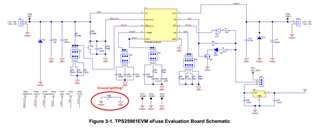
(1) Ground Splitting:
As per the EVM, the ground is split into power ground and IC ground and connected together through 0 Ohm 0603 Resistor. However the datasheet doesn't not highlight this information. Is ground splitting really necessary?
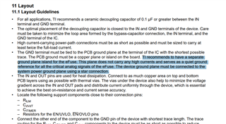
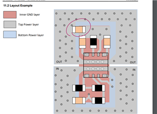
(2) Layer Stackup Requirements and Layout Guidelines:
The layout images mentioned in the EVM seems to be incomplete with only 2 layers (top and bottom) shown. However, the datasheet recommends a min. 4 Layer stackup with the ground planes routed internally.
It would be helpful if design files of the TPS25981EVM could be provided for analysis and understanding of the layout requirements for this IC.
(3) UVLO & OVLO Resistor Settings:
There are two configurations mentioned in the datasheet and EVM,
Config (a): using individual resistor divider networks on each UVLO and OVLO pins from the IC (from EVM)
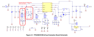
Config (b): Using a stacked Resistor divider connecting both UVLO and OVLO Pins. (from Datasheet)
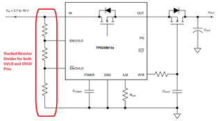
Kindly provide clarity on which out of these has merit over the other.
Regards,
Shashank K S
Electronics Engineer