This thread has been locked.

If you have a related question, please click the "Ask a related question" button in the top right corner. The newly created question will be automatically linked to this question.

UCC5390: SIC gate driver design questions.

Part Number: UCC5390
Other Parts Discussed in Thread: UCC5350, UCC5310,

Tool/software:

I hope you are doing well.

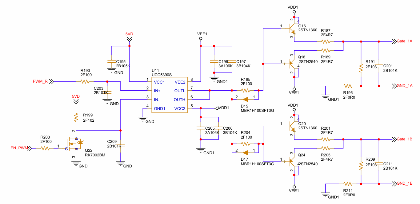
I have designed an FET drive circuit using the UCC5390S, but I am currently experiencing significant FET ringing and am seeking a solution.

  1. I am considering removing the push-pull circuit. Could you kindly confirm whether the UCC5390S is capable of driving two FETs? The datasheet indicates a sink current of 10A.
  2. I believe that using the UCC5350M Miller Clamp IC could help mitigate this issue. However, would I need to use one IC per FET?
  3. If you have any additional recommendations for resolving this issue, I would greatly appreciate your advice.

Thank you in advance for your support.

Best regards,


  • Hi Tae,

    High-side FET ringing is a combination of high-side parasitic drain inductance, phase capacitance, and the transconductance of the high-side FET. You can slow-the turn-on speed of the high-side FET by using lower drive strength or adding gate resistance, but this is a very energy in-efficient approach.

    In my designs, I am able to use electrolytic capacitors on the supply rail that are able to provide enough series resistance to dampen the LC tank below resonance.

    A more expensive but more common solution is to use a SiC FET, which has lower transconductance. These devices have 1/10 the gm of normal silicon FETs when they are passing through their saturation region (Vds rise time) when turning on. You can also use a cheaper, higher Rdson version of your existing silicon FET. Basically what you are trying to avoid is making a parasitic Colpitts oscillator when your high-side turns ON:

    Colpitts Oscillator:

    Also, if you have a BJT totem pole output buffer, you don't need such a good gate driver (17A). You can use the UCC5310 (2A), since the output stage is buffered, the internal output stage is not important. If you forgo the BJT totem pole, then you should use a UCC5350 or UCC5390. A UCC5310 would work also; it would be equivalent to using a higher external gate resistor with a stronger gate driver.

    Do you have any waveforms of your switch node? I can help you come up with a dampening circuit based on the frequency of oscillation. And I will have to know the FET part number.

    Here is a comparison of turn-on resonance in the same exact circuit with a Si FET (STW78N65M5) vs. a SiC FET (C3M0015065D) with 5Ohms gate resistance and the UCC5350:

    Silicon FET:

    Silicon Carbide FET:

    Best regards,

    Sean

  • Thank you for your response.

    The waveform below shows the FET gate-to-source (G-S) signal (C3).
    I am currently using an SiC FET, specifically the IMZA65R015M2H (Infineon).

    Additionally, if I remove the push-pull circuit from the schematic, would it be possible to use the UCC5350M instead?

    I would appreciate your advice on this.

    Best regards,

  • Hi Tae,

    If this is already a SiC FET, the next step I recommend is to revisit your a high-voltage decoupling network to dampen the supply ringing. The supply is shorted to the switch node when it is ringing.

    You can certainly pin-to-pin swap the UCC5390 and the UCC5350. However, UCC5390 is a stronger device.

    -Sean