This thread has been locked.

If you have a related question, please click the "Ask a related question" button in the top right corner. The newly created question will be automatically linked to this question.

LM5176: Cycle skipping and ringing waveforms; poor efficiency and boots into two modes.

Part Number: LM5176

Tool/software:

Hello to all.

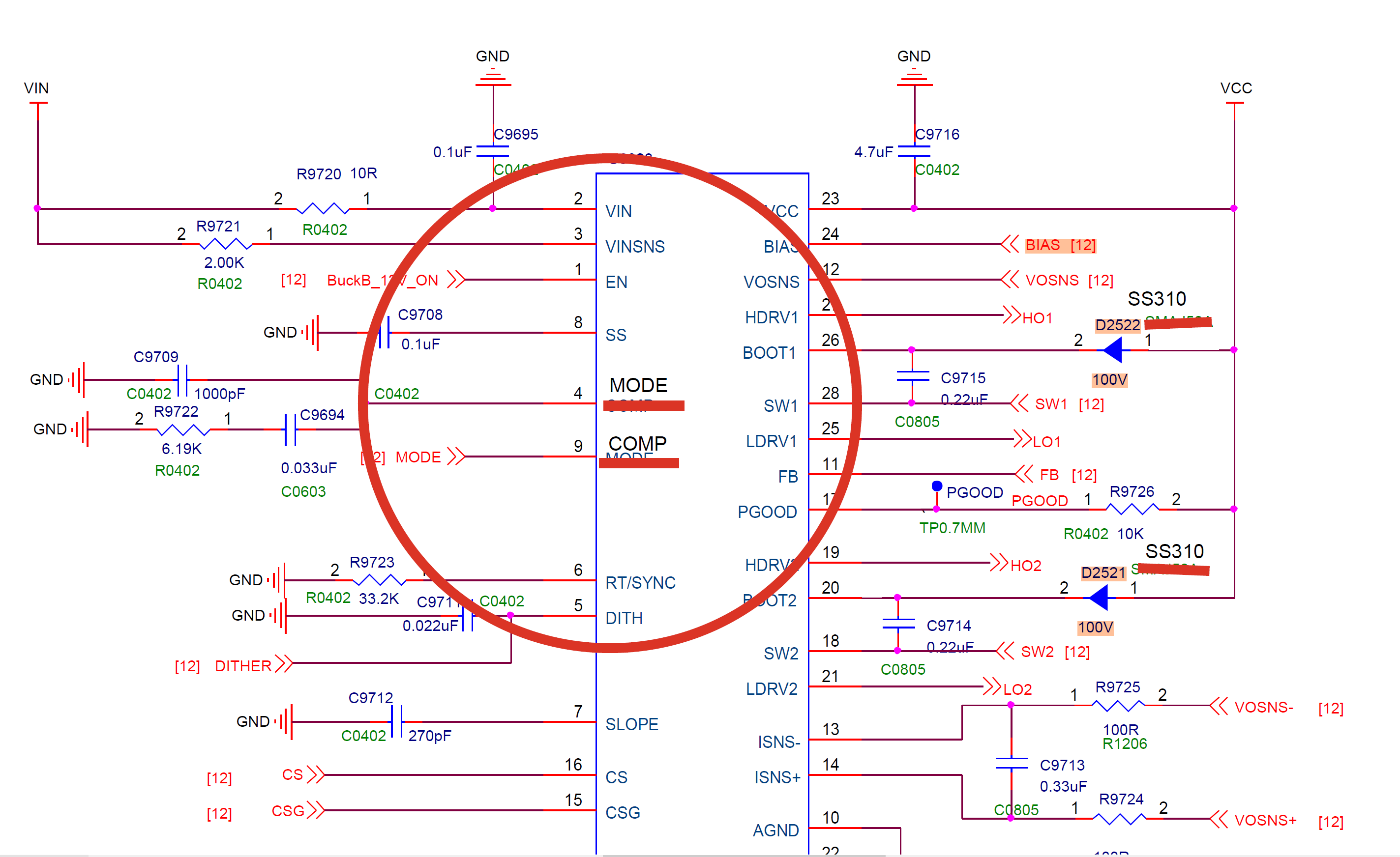
We are implementing an LM5176 for a router motherboard application.

The basic specifications are:

Vin = 8V-36 

Vout = 12V

Imax = 6A

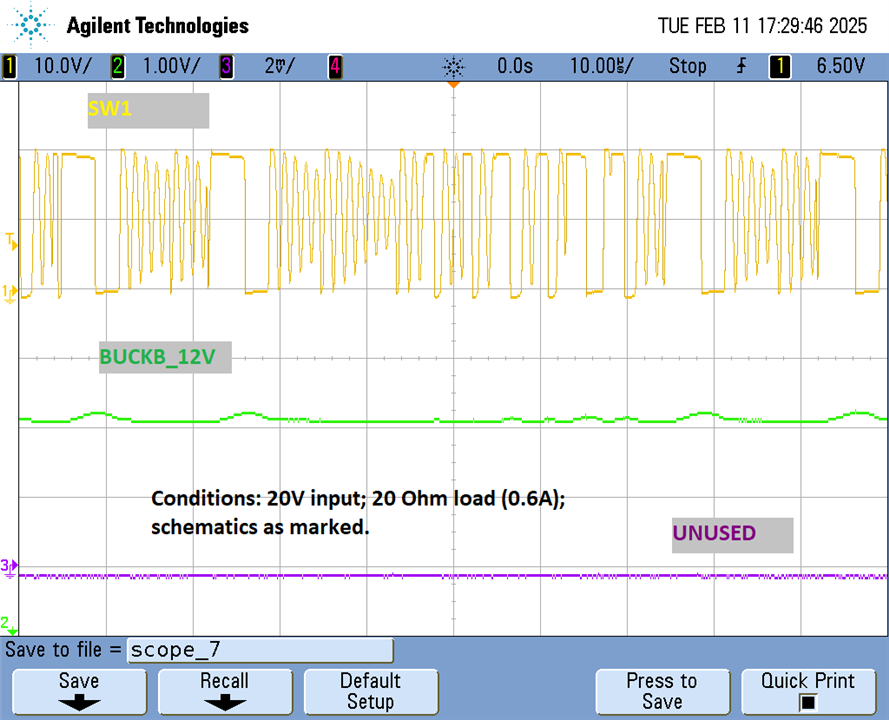
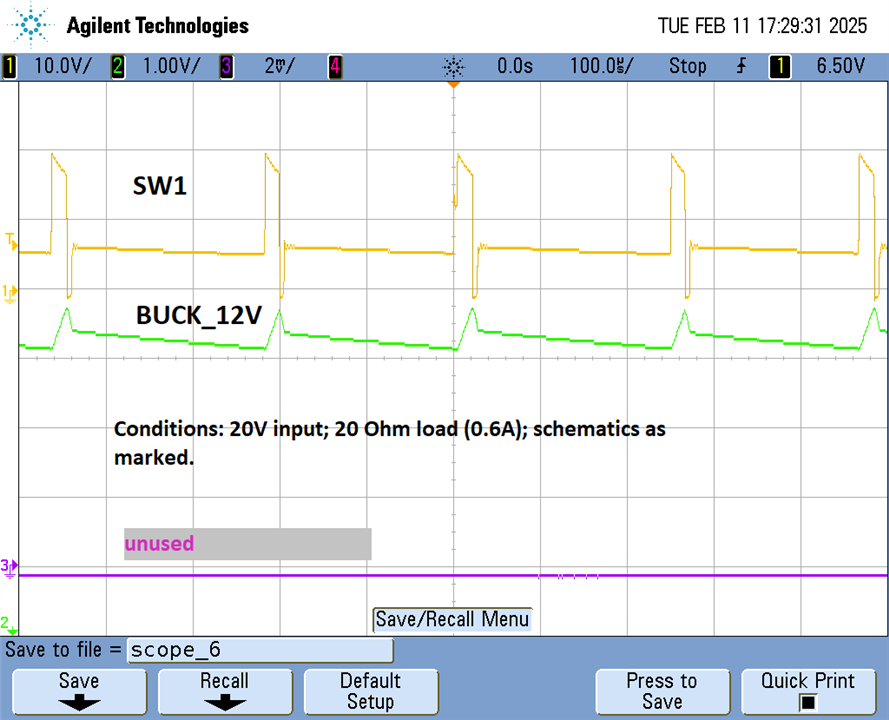
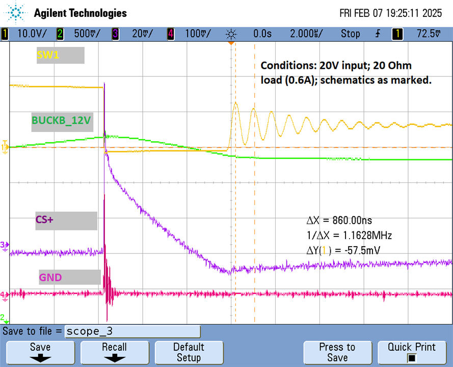
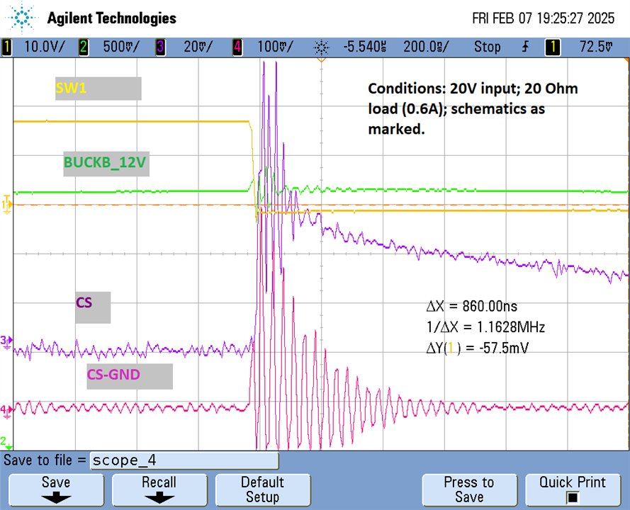
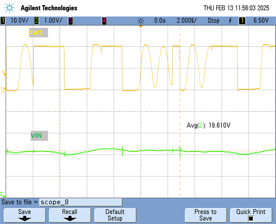
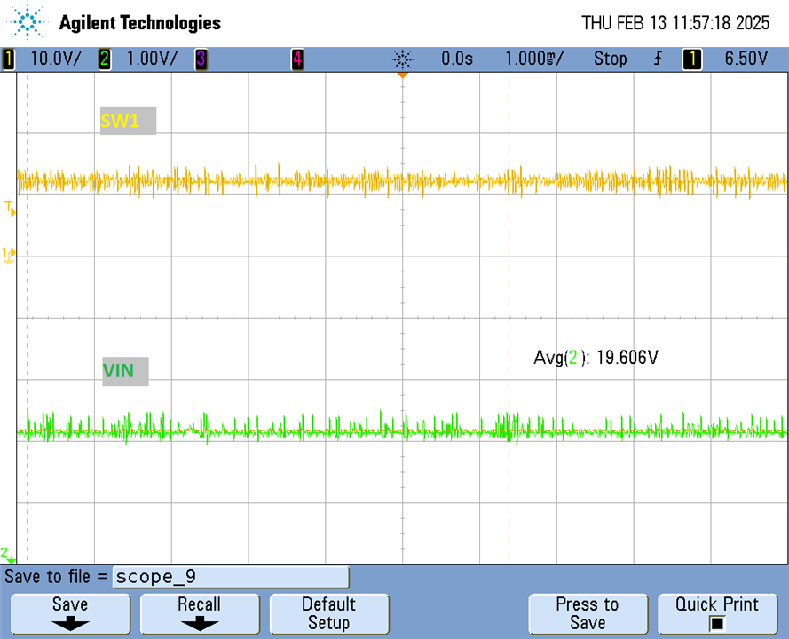
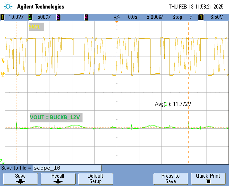
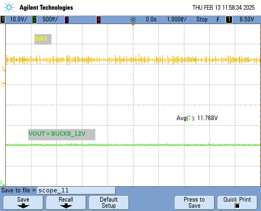
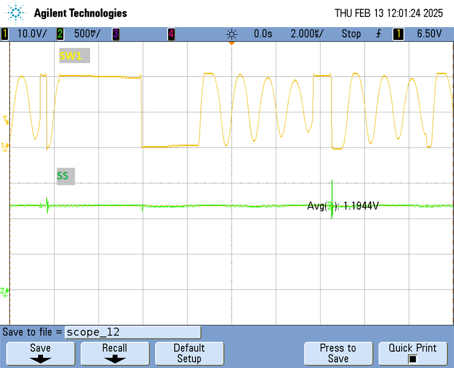
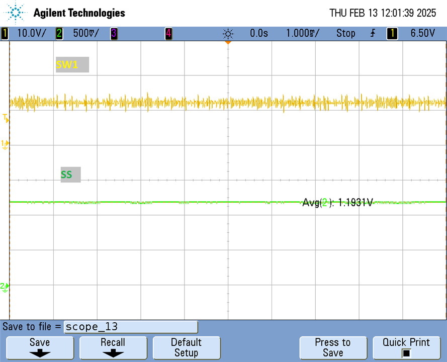
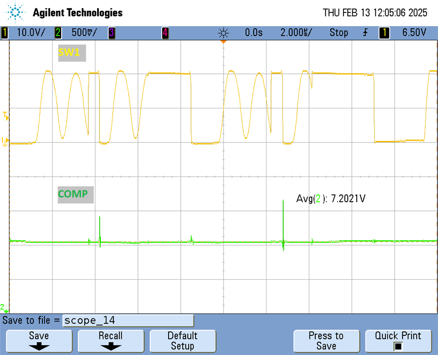
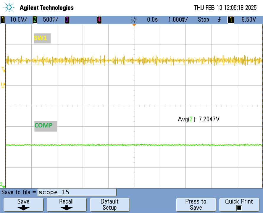
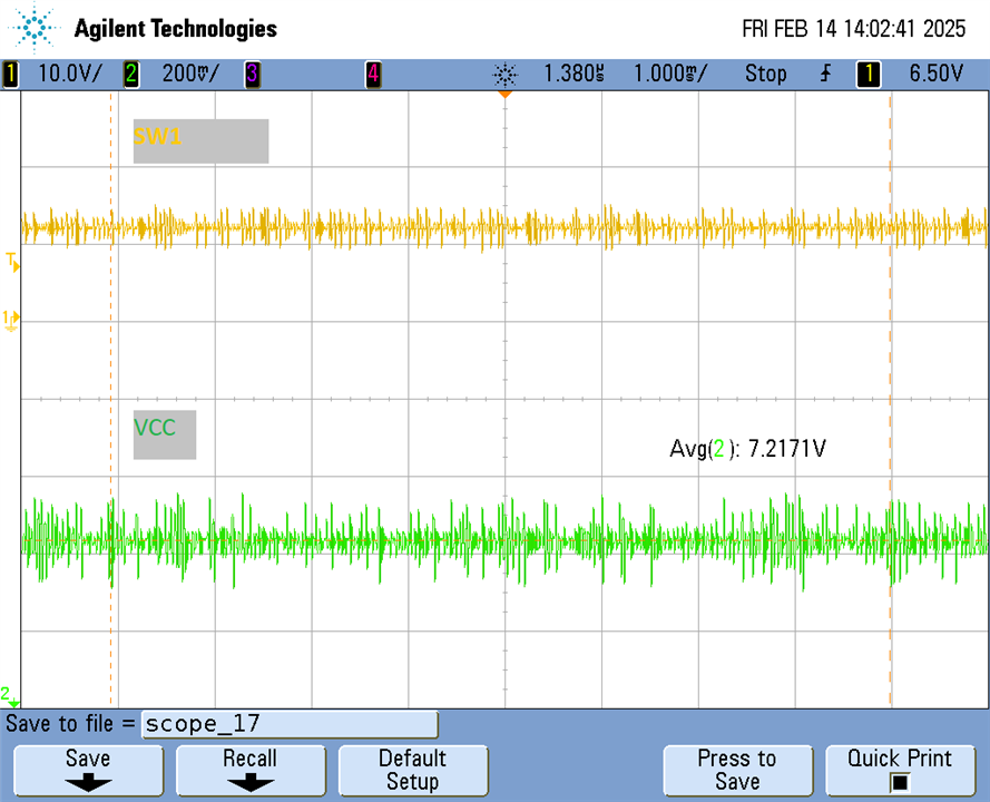
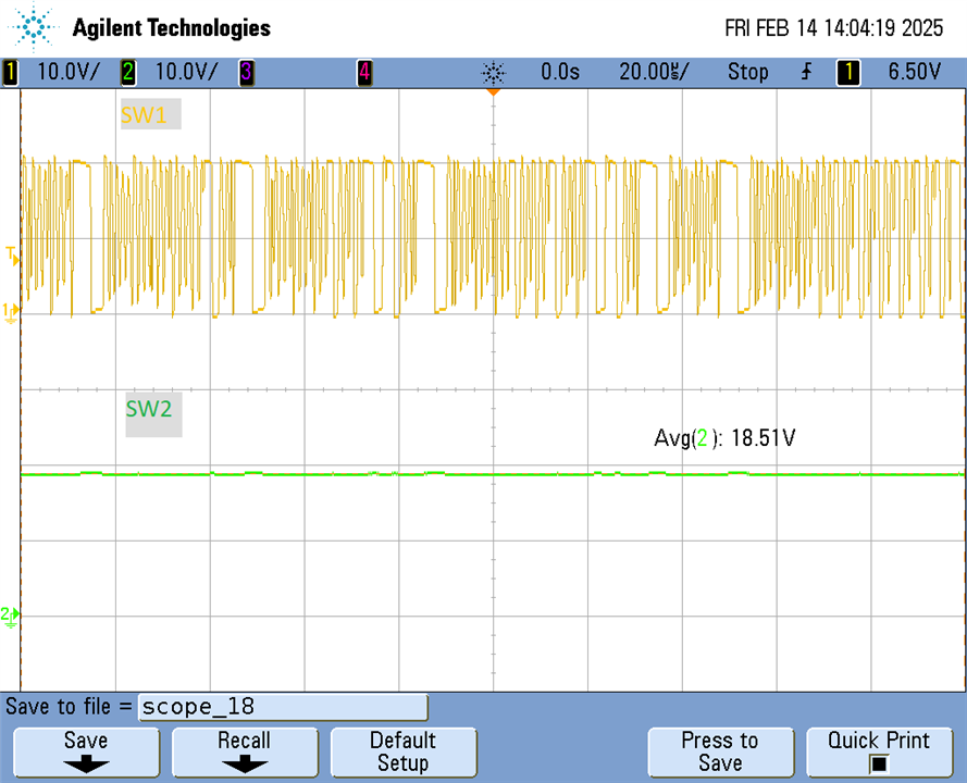
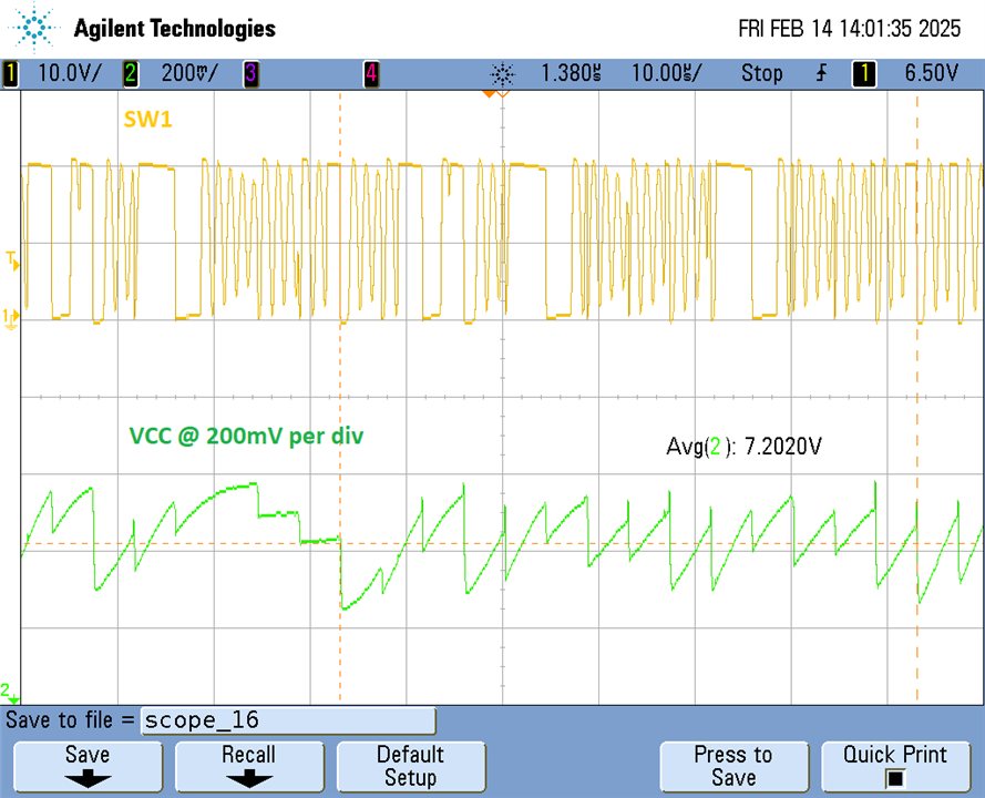
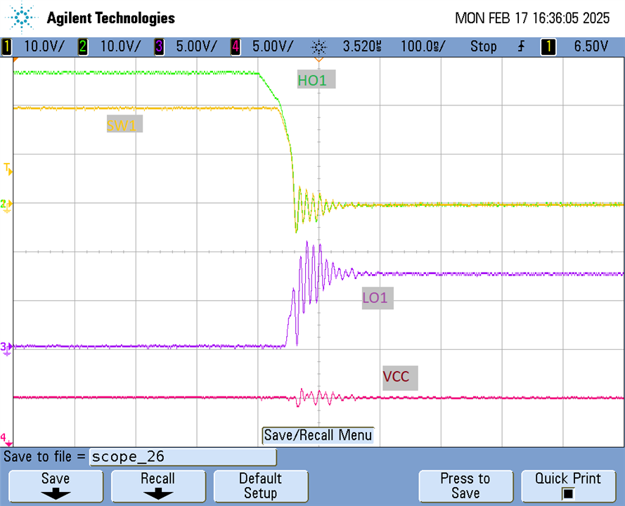
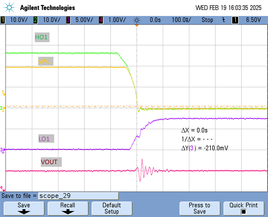
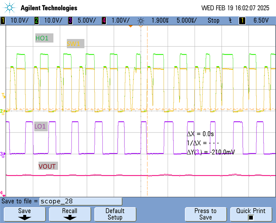
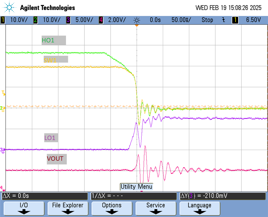
I have a first article board, and there is one other board that is currently in-use. Originally, we had startup issues and problems operating in Boost mode. We do not have a diode prior to the Vin pin, so I disabled Bias feedback by setting its input to ground. That cured the boot and low-V issues, and we seem to have good Vcc under all conditions.

The issues are that the controller seems to be regularly cycle-skipping and (in one startup mode) ringing considerably between cycles. This seems to be a period where all switches are opened. We are not currently instrumented to observe the inductor current. We were able to use a Z0 probe (950 Ohms into a coax into a 50 Ohm terminator, 200x probe) which was soldered to the current sense resistor. The low-side current sense waveform looks ok, but one can observe significant ringing when the high-side switch turns off. (This could also be ground bounce.)

    LM5176 Files.zip

  • Hi Kelly,

    Thank you for using the E2E forum.

    So you have actually two boards which work with different behaviors - right?

    When you did this tests what load do you have on the output?

    Do you see this with now load, light load and/or full lood.

    Can you probe VIN, VOUT, SS, COMP for a few switching cycles and also for ~ 10ms.

    I am also not sure about the issues you had at the beginning and why putting BIAS to GND did help.

    Best regards,

     Stefan

  • Hi Stefan,

    I appreciate the help. 

    The two boards had the same initial issues. These include intermittent starting and only being able to regulate at higher input Voltages. Both boards were initially configured to use the output Voltage as Bias for the internal Vcc regulator, however there is no diode in series with the Vin input. I modified one of the boards to remove Vout from the Bias pin and instead connected it to ground (per data sheet). This solved the intermittent start issue and now we are able to operate (not well) over the full input range.

    When the tests were performed, the output was connected to a 20 Ohm, 5W power resistor. 

    We see the issues over a full range of loads (very-light load, 0.6A and 4A have been tested so far).

    Please see the attached scope shots for the requested signals. Please note that 'BUCKB_12V' is the same net as VOUT in the data sheet. (See below).

    My hypothesis on initial startup issues due to Vout on Bias, is that low input Voltages were sufficient to generate an appropriate output Voltage (12V) and that Voltage level fed back current through the body diode of the input regulator. In turn, this caused the high-side charge pump to not operate correctly. I'm not sure about this either. The regulator seems to be operating correctly (see new scope shots, for example).

    I also included schematics and layout information in the attached zip file. Not sure if you were able to retrieve it.

    Regards,

    Kelly C.

  • Hi Kelly,

    thank you for the additional info.

    First of all it shows the the controller is running stable (COMP settled) and that it does not continuously restarting (SS stable at 1.2V).

    You are right the BIAS can feedback voltage to the VIN pin, so if you VIN starts very slowly and as you do not have set and UVLO threshold (UVLO connected to VIN with only a Zener to set the level at 3.3V).

    I am not sure now if I have understood your issue or what you think is not OK.

    So if there are periods where all 4 switches are open, this typically when the output rises to high and the controller detects and overvoltage on the output.
    In this case it stops operation until it has settled back again.
    Note: as you now have a diode in the input the controller can not push energy back to the input to get the output voltage down.

    PS: Schematic as in the zip file but not the layout.

    Best regards,

     Stefan

  • Hi Stefan,

    Yes, confirmed that we are not currently using UVLO, we are using a logic output from an over-Voltage chip that precedes the LM5176. The 3.3 Zener is not populated (DNP). There is currently no under-Voltage detect, which is a problem that needs to be addressed. I can temporarily enable this locally to the LM5176 locally, at least until a better fix is available. 

    Regarding the issues: Based on your explanation of the overvoltage lockout, this behavior is causing significantly increased ripple on the input and output Voltages. The SW1 waveform does not match the EVM plots, which are more like duty-cycle square waves. (This design is based on the EVM design.) The converter is supposed to operate in CCM. These cycle-skipping switch waveforms persist at higher load currents, also in Boost mode, and are affecting the efficiency. So, how do we fix this?

    Secondly the converter boots into two different modes: by this I mean that the SW1 are very different under the same input conditions when powering off and on again (even if waiting for settling). This is shown in the first two pictures above. Maybe UVLO would solve this?

    Sorry for lack of clarity. The scope shots are based on the schematics as marked and uploaded. There is currently no diode in the Vin path. Instead, the Bias pin is set to ground. Accordingly, there is now (to my knowledge) no reverse-current through the internal regulator body diode path. IMO, this reverse current is not 'normally intended operation'. Is it necessary to have Bias connected to the output for normally intended operation in Buck mode (to be in 100% CCM)?

    So, is the overvoltage issue a lack of fast feedback from the current sense? Is there a problem with current sense or slope comp?

    Attaching the missing layout file.

    Best Regards,

    Kelly C

    .Layout with Assy.pdf

  • Hi Kelly,

    I will try to have a closer look into the layout but this might take some time as the response of the pdf reader is super slow when I try to work with this file.

    What i have seen is that the ratio of input to output caps is very large. As mentioned it looks like the controller detects over voltage on the output. As the output caps are much higher then the input. Now as controller tries to shift energy back to the input and the cap size there is very small the input voltage gets pushed up (which can be seen in the scope plots). 

    So please try to add some bulk caps also on the input side.

    I also have seen that the cap on VCC is 0402 size. Have you checked the DC BIAS behavior of this shunt? What is the effective capacitance of this cap at 7V?

    Best regards,

     Stefan

  • Hi Stephan,

    The pdf layout file loads quickly here-we can bring up a new page in much less than a second. If you need the pages separated, we can do that here. Maybe try screen printing?

    There is a bulk capacitor of 100uF on the input, as well as 7x 4.7uF caps to reduce the ESR at higher frequencies. This is the same configuration as in the EVM. I will try a parallel 100uF to see if helps.

    The ratio of output to input capacitance is the same as the EVM, Figure 22. I'm not understanding why higher caps cause an over-Voltage at the output. Please try and explain this more clearly. We are in full Buck mode, there is no current path from the output to the input when the high-side switch is off. When the high-side switch is on, the current flow is from input to output, 19V vs 12V. So, I don't understand how energy can shift from the output to the input. Attached is a scope shot of SW2, which shows that the Boost FETs are not switching.

    By color, the VCC cap is estimated to be X7R or X5R. I will need to inquire from our design partner to find out its technology and Voltage rating. I can also try to swap it with known-good technology and see if it helps. However, I see less than 400mV of ripple on VCC, so it should not create any issues enhancing the FETs (see scope shots). I suspect that this ripple will reduce when the SW1 waveform is in compliance. Is there a ripple requirement for VCC?

    Please comment on this question: Is there a problem with current sense or slope comp?

    Regards,

    Kelly C.

  • Hi Kelly,

    yes, would be better if you can provide separated pdf files - it will make it easier to overlay them.

    Sorry, did not see the 100uF input bulk cap in the schematic.

    The issue might be related to an problem with the current sensing circuit. This could be due to the layout but also the used current sense resistor (esp. inductance) can make issues.
    Here esp. the ringing you see in the second scope plot in the first thread looks to much. I still do not understand why this is behaving different on startup but might be some temp. dependency.

    So reviewing the layout would be a good next step.

    You also can try to replace the used shunt resistor with another one:

    E.g. use two in parallel with the double resistance 

    or use one with the terminals on the lonb side.

    Best regards,

     Stefan

  • Hi Stephan,

    We tried adding an input cap in parallel with the 100uF (220uF, AE hybrid, 25V). There was no change in the ringing issues.

    We replaced the 0603 capacitor on the output of the Vcc regulator with a 10uF, 0805, 25V, X5R. It did make a noticeable difference in the Vcc ripple Voltage - reduced to around 150mV from around 400mV. It did not affect the ringing issue, but I will recommend a design change or component swap. I notice an 0201 capacitor on the VOSNS pin. I will investigate this and probably recommend an upgrade.

    We changed the CS resistor to two 8 milliOhm 2512 resistors piggybacked. It didn't make a noticeable difference in the ringing issues or CS waveforms. 

    Attached are the layout pdfs in individual files.

    I'm wondering about shoot-through since there is so much noise produced on the falling edge of high-side switch. One thing we noticed is that the FETs are the same Part Number for high-side and low side FETs. This does differ from the EVM that used different devices for the low side FETs. Maybe this is a switching speed issue? I'm setting up to look at the gate drives, simultaneously.

    Regarding the OVP based on the output Voltage, it does appear that the output Voltage is spiking over the OVP limit and apparently the switches are turning off. However, we don't see activity on the PGOOD pin. That seems contrary to the data sheet. Is there integration on the PGOOD trigger?

    Best Regards,

    Kelly C.


    Layout Pdfs.zip

  • Hi Kelly,

    will review the layout but as you showed that the VCC cap had an impact, please share the DC BIAS derating of the first used and the new used capacitor.

    (Part number of both caps could help as well)

    Would like to check this parameter as well.

    Best regards,

     Stefan

  • Hi Kelly,

    For the layout:


    Would be much easier if all layout plots would have the same scaling and same position.
    This way it is very hard to overlay and follow traces.

    Can you provide layout plots where this current loops are highlighted
    - HDRV1 -> MOSFET - SW1 -> LM5176
    - HDRV2 -> MOSFET - SW2 -> LM5176

    GND connection of AGND and PGND pins

    Are there high current paths in the GND plane below the LM5176 - is so a AGND polygon iland would be recommended.
    Common conntection point between AGND and PGND could then be the thermal pad.

    MOSFET Drive signal lines are quite thin. Note this have high dI/dt signals.

    Filter for current should be close to the input of the controller to avoid noise injected into the lines get to the controller.

    Connect VCC cap also to PGND pin directly

    Best regards,

     Stefan

  • Hi Stephan,

    Attached is a screenshot with highlighted traces. The gate lines run mostly on the bottom layer. The lengths around 40-45mm.

    Attached are two screenshots of the ground pours. There is a continuous ground pour under and around the chip. The AGND and PGND pins are connected to the thermal pad under the chip. The second screenshot shows the vias-for some reason the thermal pad was blocking the view.

    The MOSFET gate drive traces are 5 mils. I agree that they should be wider. However, I don't see an impact on the existing functionality. There shouldn't be a trace power issue due to duty cycle, and I don't expect much difference in inductance by increasing the width. 

    I'm not sure which 'filter for current' you are identifying. The gate signal current is sourced by the Vcc cap (C9716), which should be ok now (see attached scope shot). Gate current is also sourced by the boot caps C9714 and C9715 which are fairly close to the LM5176, given their relative size. That all looks ok to me. I may not be following you here.

    VCC cap is connected directly to PGND via a fat pour - thankfully, that's how I was able to shoehorn an 0805 in there!

    I ran a scope trace with the HO1 and LO1 gate drives for the Buck FETS. The ringing that I see on the ground seems to be on the low side. I was previously mistaken about the EVM FET configuration. The EVM has the same FETs on the high and low side of the Buck side that we have now. It's the Boost side that has different FETS. Anyway, we see ringing on the LO1 line and the Vcc line seems stable, so I will try and adjust the gate resistor to dampen it. The ringing seems to be "Miller effect". The high-side gate drive looks OK, but maybe a little bit slow for some reason.

    I put a request with the customer to ask our Design partner for an updated BOM. The Vcc cap is PN CL21A106KAYNNNG. The derated capacitance at 7.5V is 4.5uF, seems OK (see plot). (rated at 10uF, 25V, X5R, 0805)

    Best Regards,

    Kelly C.

  • Hi Kelly,

    This is the new Cap -right? In the initial schematic is say 4.7uF
    So it de-rates at 7V by 70% and would give ~ 3uF - so should be OK.

    You are right the is quite a lot of ringing on the SW node and also the low side gate. This should be fixed.
    This might be due to a too high inductance of the high side gate line and therefore does not ramp down as fast as the SW node. This can lead to a reopen of the high side MOSFET.
    You can try to add an external capacitor between Gate and Drain (2-3 times of the gate drain capacitance or start with 1nF).

    But I do not think that this is the issue for the for starting up into different modes but can for sure have an impact on the efficiency.

    Best regards,

     Stefan

  • Hi Stephan,

    Well, if you're doing worst-case analysis, then you have to figure also the cap tolerance, degradation due to soldering and long-term ageing. (humor)

    We tried 1nf, 2.2nf and 10nf. It wasn't until we got to 10 nF to get some major improvement. Three plots attached (reverse order):

    * First plot is 2.2nF, 2nd plot is 10nF wider time span, then 10nF zoomed. 

    The behavior is improving. The cycle skipping is still occurring, but only one-two cycles are skipped now. At this capacitance level, we're concerned about switching losses-but we should 'get it working' and then optimize later. We ordered some 0402 gate resistors in different sizes - we can try this in a couple of days. The SW1 falling edge seems to have a large impact on the Output Voltage.

    What are your thoughts on how to proceed next? The capacitance level already seems a bit high.

    Best Regards,

    Kelly C.

  • Hi Kelly,

    thank you for your extensive testing. 10nF is really quite high and i would not have expected that this high cap would be required.

    On the other hand this also gives a hint that the inductance on the gate lines for the high side MOSFET (esp. in this case) could be to high.

    Keep in mind that width of the routing has an huge impact here. Also the return path of the gate line of the high side MOSFET is the SWx node.
    Both lines are impacting this connection. To keep the inductance small also the area build by this two lines should be as small as possible. The best is to have both on top of each other.  I will add below some additional info on the layout.

    Additional info on layout can be found here :

    (1) Four-switch buck-boost layout tip No. 1: identifying the critical parts for layout

    (2) Four-switch buck-boost layout tip No. 2: optimizing hot loops in the power stage

    (3) Four-switch buck-boost layout tip No. 3: separating differential sense lines from power planes

    (4) Four-switch buck-boost layout tip No. 4: routing gate-drive and return paths

    Best regards,

     Stefan

  • Hi Stephan,

    I added #30 wires to the boost gate drives, both HI1 and LO1. Roughly, I routed them over the existing traces; I left the existing traces in. Regarding inductance, the additions are approximately equivalent to using a 25 mil trace. They are each about 40mm long. Total inductance per wire is probably reduced to around 15 nH. There was no change in the waveforms. (I was hoping that the high-side would speed a bit.)

    Thanks for all the layout info. It should be mute, as the intent was to copy the EVM design, which is on me for not enforcing this. The question now is if we scrap the current layout, or can we make it work with beefed up gate drive traces, increased capacitor sizes, and some minor corrections in the routing? Unless I can prove it working with board modifications, we will need a reroute. Any ideas on this would be helpful.

    Regarding the two modes of startup: now that waveforms are somewhat improved, the modes follow a consistent pattern. When I first start up, the low duty-cycle mode appears (third scope-shot from the top). When I restart, the continuous pulsed mode appears (two scope-shots up from here). Probably the bulk capacitance is not sufficiently charged when the controller starts up initially. Since we do not have UVLO enabled, this could be due to low input Voltage. I can try a longer SS period and also figure out how to enable UVLO in cooperation with the existing Enable from the protection chip. Other ideas?

    I will also incorporate a diode and then turn the Bias back on to test it.

    Best Regards,

    Kelly C.

  • HI Kelly,

    for the UVLO control you could add the resistor divider from VIN to GND to set the UVLO level and then just pull the UVLO/EN signal to low via a Diode which is connected to the controller. (like an open collector/drain circuit).

    Best regards,

     Stefan

  • Hi Stephan,

    I found a pinout issue. Comp and Mode pins are reversed. I saw that the comp pin was inactive, and further it was outside its abs max. Since the unit was regulating-I scratched my head awhile and found it. The waveforms are 'normal' and the startup issue seemed to disappear as well. The startup circuit needs some work-it's already set up to implement the UVLO if we add a resistor to ground, but there is another issue regarding a logic translator that's on the same input signal.

    I'm rechecking the gate drives, since the efficiency is reduced because of the large gate resistor. 

    Cheers,

    Kelly C.

  • Hi Kelly,

    thank you for sharing - good that you have found this.

    Please let me know if there is any other issues or questions where I can assist.

    Best regards,

     Stefan