This thread has been locked.

If you have a related question, please click the "Ask a related question" button in the top right corner. The newly created question will be automatically linked to this question.

BQ2982: Wrong output level on DSG and CHG pins

Part Number: BQ2982

Tool/software:

Hello,

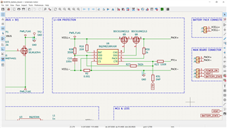
we have design a BMS PCB board for lithium-ion protection (1 cell) with BQ298218 chip.

Unfortunatelly, output pins of the chip aren't able to drive the MOSFET on the PACK + line (with VCELL voltage = 4V, CHG voltage around 4V and DSG is around 2,5V), wich cause a big voltage drop out on output.

Here the schematics, is there anything wrong with our implementation (for the test, the CTR pin is pull down to GND) ?

  • Hello Tristan,

    I will get back to you by tomorrow. Sorry for the wait! 

    Best Regards,

    Luis Hernandez Salomon

  • OK, waiting for you !

    Thanks

  • Hello Luis, 

    I have debugged a little more and here more precise pproblems:

    Voltage on CHG pin is ok and can open/short the MOSFET. Voltage on DSG is never higher than battery voltage, wich, i think, cannot turn on the DSG  MOSFET. What is strange is there is always voltage on output, even when the CHG MOS is off. Is this behaviour normal ? Can you help me please ?

    Thanks

  • Hello Tristan, 

    Sorry for the wait! Very busy week and we had U.S. holidays yesterday.

    Did you power the device? This can be done by either applying a charger voltage, or by shorting BAT to PACK+ briefly. 

    Best Regards,

    Luis Hernandez Salomon

  • Thanks for your reply. The problem was a damaged MOSFET. Everything works now. 

    But if i understand well, this BQ is done to be powered by a charger only, it cannot supply a load by itself if no charger are connected to PACK+ pin?

    Our application is a portable batterie pack: it can be uncliped from device and be recharged, or it can be clipped to the device and supply it without any charger connected. IT can be either clipped to the device, supppliying the device and be connected to a charger at the same time. I am thinking this IC is not suitable for our application. Can you confirm my opinion ? If i am right, can you advise me a protection IC with a control input pin that fit our application? 

  • Hello Tristan,

    Glad it all works Slight smile.

    When the part enters SHUTDOWN it requires a voltage on the PACK pin to get out of SHUTDOWN. This is usually done with a charger attachment. In some cases customers may have a switch between BAT/PACK+ so there's a brief voltage to turn-on the device.

    Best Regards,

    Luis Hernandez Salomon

  • OK, thanks for your answer, 

    But when i don't have any charger connected to PACK+, and if i short BAT and PACK+, voltage on PACK+ decrease instantly after the short removal. Is it the normal behaviour ?

  • OK, found the issue, CTR input wasn't propoerly grounded. Thank for your time, everythings is OK