This thread has been locked.

If you have a related question, please click the "Ask a related question" button in the top right corner. The newly created question will be automatically linked to this question.

TPS54620: Loop stability compensation

Part Number: TPS54620

Tool/software:

Hello,

Question for below:

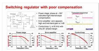
1) In the error amplifer, how to read the phase margin? I suppose it should go to -180, but it's not.

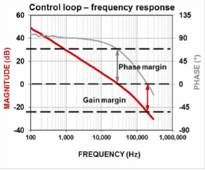
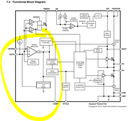
2) For the control loop, what's specfic in schematic? I suppose it should be the same as error amplifier.

3) For the control loop, why the margin is 20degree? If compared with -180degree, the margin should be much bigger.

开关模式电源转换器补偿简单易行 | TI.com.cn

  • Hello Pan, 

    below shows a good example on how to read phase margin, gain margin and Fco (BW). 

    1) from the slide that you showed, looks like the error amplifier is at ~135deg

    2) The systems they shows is under dumped and it is unstable with poor compensations 

    3) for stable systems should be at least 45 deg or more 

    Thanks! 

    Tahar

  • 1) from the slide that you showed, looks like the error amplifier is at ~135deg.    [LP]  -135deg is margin, right? Why the TI traiing material (pic I attached) call 20degree margin.

    2) The systems they shows is under dumped and it is unstable with poor compensations [LP] My question is which part you call controll loop? Please give me mark up drawing on TPS54620 block diagram.

  • Hi Liping,

    The slide attached is for the control loop only which is what you typically measure near the FB pin of the device. That slide is showing Phase margin = 67.5°  and Gain margin ~23dB. This tends to be measured above top FB/VSENSE resistor.

    As far as the control loop, that typical involves any components that affect output regulation:

    TPS54620 offer external compensation to alter stability through COMP pin.

    Regards,

    Eileen