This thread has been locked.

If you have a related question, please click the "Ask a related question" button in the top right corner. The newly created question will be automatically linked to this question.

LM5122: Question about LM5122MHX/NOPB

Part Number: LM5122

Tool/software:

Hello:

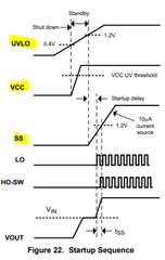
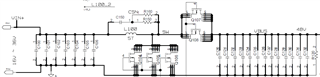
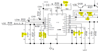
The following figure is the schematic diagram of the specific application peripheral circuit of the LM5122MHX/NOPB chip. The input voltage VIN+ is stepped down and stabilized by LDO to output VCC (10v) to power the chip. The input voltage VIN+ is connected to the chip CSP pin through the R151 (10kohm) resistor. The chip VCC (10V) is powered normally, and the UVLO pin voltage is divided by 1.5V (satisfying greater than 1.2V).

The current fault phenomenon is:

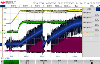
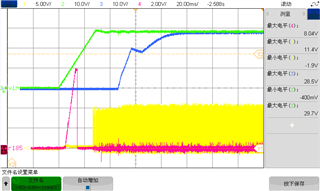
1. At room temperature, under different VIN+ rising slopes (VIN+ rises from 0V to 28V), the chip works normally and LO is driven. The following figure shows the test waveform of VIN+28V input at room temperature (the rising slope is 1V/ms, that is, VIN+ rises from 0V to 28V in 28ms). The green CH3 channel is the VIN+ rising waveform, and the yellow CH1 channel is the LO waveform.

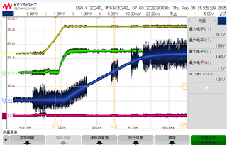
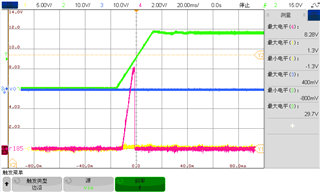
2. At low temperature of -40℃, when the input VIN+ rising slope is 1V/ms (i.e. VIN+ rises from 0V to 28V in 28ms), the chip works abnormally and LO is not driven. The following figure shows the test waveform of low temperature of -40℃, input VIN+28V (rising slope is 1V/ms, i.e. VIN+ rises from 0V to 28V in 28ms). The green color of CH3 channel is the VIN+ rising waveform, and the yellow color of CH1 channel is the LO waveform.

Please help analyze the following problem: The chip does not work at low temperature, in a specific input slope range, and the explanation of the mechanism

  • Hi Jimmy,

    Thanks for using the e2e forum.

    So the device starts up normal at room temperature, but stays in shutdown mode during the same test at -40C.
    If the device does not start switching, it would make sense to check if all conditions for start-up are met.

    Could you do a new test measurement and check the signals for UVLO, VCC and SS?
    If one of these voltages does not rise, it would explain why the device does not start switching.

    Would you also be willing to share the schematic part of the power stage? (inductor, MOSFET, input/output caps)
    In Boost topology, the VOUT should follow VIN if the device is inactive. This does not seem to be the case in your waveforms if the blue curve is VOUT, so I want to make sure I am not missing relevant information about the design.

    Thanks and best regards,
    Niklas

  • Hi Niklas:

    1. The main power circuit schematic diagram is shown in the attached BOOST power circuit diagram. The specific parameters are the total input capacitance of 59.4uF, the total BOOST output capacitance of 61.1uF, and the inductance of 2.8uH;

    2. The VCC, UVLO, SS and LO drive waveform test results that meet the startup conditions of the chip are shown in the attached Figure 2 (normal temperature 25℃, input VIN+28V, slope 1v/ms) and Figure 3 (low temperature -40℃, input VIN+28V, slope 1v/ms).
    --According to the test results, at low temperatures, VCC, UVLO, and SS meet the startup conditions, and LO has no drive signal.

    Figure 2

    Figure 3


    The VCC waveform was tested before, and the power supply of 10v was normal, and the UVLO of 1.4v also met the startup conditions. It was also suspected that the UVLO margin was insufficient, resulting in no startup. Later, we adjusted the peripheral voltage divider resistor and increased the UVLO to 1.8v. The chip still did not drive at low temperatures.

    In addition, there are currently multiple chips with this type of anomaly. Please help analyze the problem and determine whether the conditions for further FA analysis of the abnormal chip are met. Thank you!

  • Hi Jimmy,

    Thanks for the update and the waveforms.

    This confirms that the start-up itself should not be related to the issue.
    As you say there are multiple chips with this issue, can you give me a number how many units shows this issue out of how many tests?
    Do you also see that some units can start up at -40C, while the failing units do not start switching?
    Also, can you give more details how the low temperature test is performed? Do you use a cooling chamber, or cold spray?

    Thanks and best regards,
    Niklas

  • Hi Niklas:

    1. The specific failure rate is currently being counted by customers. Currently, only the R&D side has tested 2 out of 6 chips and found this phenomenon;
    2. Normal chips can work normally at a low temperature of -40℃, and faulty chips cannot work at a low temperature of -40℃. The fault phenomenon can be stably reproduced;
    3. The low-temperature test is a cooling room (box) test. The cooling box temperature is set to -40℃, and the test is conducted after the cooling and insulation time is 2 hours.
    Since the fault can be stably reproduced, may I ask if the conditions for faulty chip analysis are met? Thank you!

  • Hi Jimmy,

    Thanks for the quick feedback.
    2 out of 6 chips is rather high, so this might still be a system issue instead of a device problem.

    As you can consistently reproduce the issue, the chip should be valid for a quality issue request.
    All information and how to set up a ticket can be found here: https://www.ti.com/support-quality/quality-reliability.html

    If a faulty unit is sent to us, we will try to reproduce the failure on our LM5122 EVM board. If we can reproduce the issue here, failure analysis will take the next steps to find the root cause. The only problem is when we cannot reproduce the failure and the IC works fine at -40C on our EVM board. Then the IC may be sent back as TNI (trouble not identified)

    As this can lose a lot of time for both sides, I would check if any optimizations of the design can fix the problem before sending in a unit.

    I can offer to review the schematic. For this I would need the value for the peak load conditions, as well as the component values marked here:

    If you are willing to perform additional bench tests on your side, I would ask if you can measure the FB and COMP signal during a failure situation.
    These define the PWM signal once startup is completed.

    Thanks and best regards,
    Niklas