


Tool/software:
Hello...
We have problem in our design as part doesn't work as expected. I have already replaced part but have same issue.
The problem is that we don't get output at all.
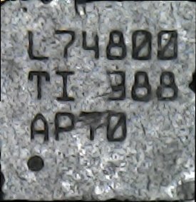
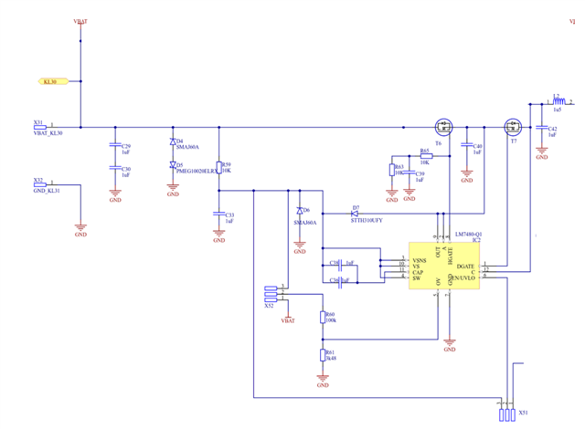
The attached is part of schematics and image of chip marking.
I have measured all voltages and here is result:
With test condition with X51 set to deliver 0 V to EN/UVLO the measured voltage at pins are:
| Item | Voltage | Our opinion |
| VBAT | 12.02 V | Supply voltage |
| VS, VSNS, SW | 12.02 V | As should be |
| OV | 0.40 V | Overvoltage not triggered (Under 1.13 V) |
| OUT, A | 0.00 V | OK as EN/ULVO is low |
| HGATE, DGATE | 0.00 V | OK as EN/ULVO is low |
| C | 0.00 V | Excepted as gate is low |
| CAP | 11.36 V | Probably ok as EN/ULVO is low |
| EN/ULVO | 0.00 V | connected to GND |
And other set of measurements with test condition with X51 set to deliver 12 V to EN/UVLO the measured voltage at pins are:
| Item | Voltage | Our opinion |
| VBAT | 12.02 V | Supply voltage |
| VS, VSNS, SW | 11.97 V | 50 mV drop on R59 indicating 5 uA power draw |
| OV | 0.40 V | Overvoltage not triggered (Under 1.13 V) |
| OUT, A | 0.00 V | Expected as GATE is LOW |
| HGATE, DGATE | 0.00 V | It should be around 20V |
| C | 0.00 V | Excepted as gate is low |
| CAP | 11.36 V | Probably wrong as charge pump should run |
| EN/ULVO | 11.97 V | connected to VS |
Really don't know what is wrong there so any help is welcome.


