This thread has been locked.

If you have a related question, please click the "Ask a related question" button in the top right corner. The newly created question will be automatically linked to this question.

LM5156H: Design review

Part Number: LM5156H
Other Parts Discussed in Thread: LM51561H, LM5156, TPS61087

Tool/software:

Hi all,

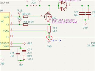
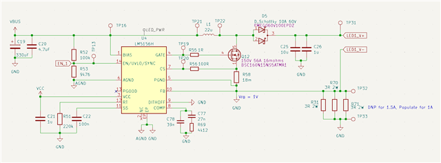
I'm developing a boost converter for LEDs, based on a Webench simulation of the LM51561H. I incorporated modifications aligned with Figure 10-9 of the datasheet to implement a low-side shunt resistor, feeding back into the control loop.

The design is for a Vin of 20-30V, and boost up to 40-50V for a current of 1A or 1.5A (deepening of the shunt populated) it also must accept a PWM on the EN_1 to dim the led

Simulation link for reference: webench.ti.com/.../SDP.cgi

I have increased the voltage rating of the mosfet to allow a voltage output of 40-50V

Despite matching the rest of the component values to the simulation, I can't achieve oscillation. Any insights into what might be preventing switching operation would be greatly appreciated.

Best regards,
OP

  • Hi OP,

    Thanks for reaching out.

    The link to your simulation does not work.

    Can you maybe attach the full link? Also i recommend to download the PSPICE model of LM5156 from ti.com and try to simulate there. There is already a boost-testbench existing.

    Best regards

    Moritz

  • Hi Moritz.

    Thanks for the reply.

    this is the link: https://webench.ti.com/appinfo/webench/scripts/SDP.cgi?ID=977A651751211E22

    I will try the Pspice simulation and share the results.

    BR,

    OP.

  • Hi Moritz,

    With the updated and calculated values, the simulation runs fine. I’m planning to hopefully test it next week.

    I wanted to ask if there’s a way to prevent the open circuit voltage from rising so high. Like an open circuit over voltage protection 

    Could any of this solutions be used?

    1. Zener Diode Clamping: a decent zener to clamp the voltage and the current.

    2. Feedback Adjustment?

    3. Crowbar SCR?

    Let me know your thoughts on this or if you’d recommend a different approach.

    BR,

    OP.

  • Hi Oriol,

    Thanks for the feedback.
    Moritz is out of office this week, so I will take over this thread.

    First off, there was a mistake in the first schematic you sent, where FB is shorted to GND. I assume you already fixed this issue as you can run the simulation without problems.

    The device should already have an internal overvoltage protection, meaning if voltage at FB rises to high (10% above target), the device will stop switching until FB voltage drops.


    If the voltage only drops at FB pin while the actual output voltage is still increasing, a zener clamping diode should be the most common solution.

    Best regards,
    Niklas

  • Hi Niklas

    It turns out that the FB shorted to GND wasn’t the issue stopping the simulation, and the PCBs we ordered don’t have this problem. i create the short afterwards and does not affect.

    Regarding the high voltage when the output is an open circuit — since it will be operating in "constant current" mode — I’m not sure if it will be able to detect the fault, given that Vled- have a low resistance to GND and will be floating from the Led+ even when the output voltage is high (if the output is at open circuit. Verified by sim).

    Maybe we could use an output voltage sensing circuit with a comparator and a flip-flop to pull EN/UVLO low if the output voltage exceeds, say, 80V.

    BR,

    OP.

  • Hi OP,

    Thanks for the clarification.

    When pulling down UVLO in case of overvoltage, you might create a hiccup behavior with Vout rising and falling close the the threshold.
    Let me get some additional feedback from within our team what would be the best recommendation to implement here.

    I will get back to you latest on Wednesday.

    Thanks and best regards,
    Niklas

  • Hi OP,

    Thanks a lot for your patience.
    I got some feedback on suitable implementations for your fault protection.
    Here is a schematic idea using a clamping diode from VOUT to FB. (Taken from the datasheet of TPS61087)

    If you are still interested in the approach of shutting down via UVLO, there are indeed some references for this as well.
    Please have a look at this article:
    https://www.ti.com/document-viewer/lit/html/SSZT626

    Please let me know if you have any additional questions on this.
    Best regards,
    Niklas

  • Hi Niklas.

    I really like the approach of the Zener. Thanks for the support!

    The Pspice sim showed a nice behaviour with a 100ohm Rz. will let you know once i try in the circuit.

    BR,

    Op