This thread has been locked.

If you have a related question, please click the "Ask a related question" button in the top right corner. The newly created question will be automatically linked to this question.

TPSM82813: Do you have any information of failure cases?

Part Number: TPSM82813

Tool/software:

Hi team,


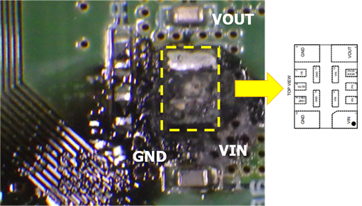
Our customer using this device and tested on the board whitch they designed.

When the test, one device was failure by burnout. From the failure occure only one case, low frequency of occurrence, we think this burnout is from damage during implementation and overvoltage mainly.

The customer want to know about other causes and information of similar failure cases using this device.

Do you have any information of similar failure cases on this device using?

Best regards,

teritama

  • Hello Teritama,

    thanks for reaching out in E2E.

    There is no known comparable failure case for this device. I agree to your assumption that this failure was most likely caused by assembly issues or over-voltage stress.

    Best regards,

    Andreas.

  • Hello Andreas-san,

    Thank you for reply. I understand your opinion.

    Incidentally, below picture is the burnout device in this case.

    Could you estimate waht block in Functional Block Diagram is broken from this?


    Best regards,

    teritama

  • Hello Teritama,

    from the picture the issue seems to be located more on the VIN side. But it is not meaningful to conclude from that, because it is a SIP (System In Package). There is an inductor on top, covering the entire device. Maybe it was no device issue at all. Maybe it was just a short below the device form soldering process. It is really hard to say.

    If it was a device damage, then over-voltage stress at VIN would be the most likely root-cause (knowing that from other older devices).

    Best regards,

    Andreas.

  • Hello Andreas-san,

    Thank you for your opinion. I would share your opinion to the customer.

    The customer find these broken device was reworked by heat gun when manufacturing.

    We think this rework can be violation Rework Guideline in below design guide.

    https://www.ti.com/lit/ug/slib006a/slib006a.pdf

    Is it correct that when the rework is violation the Rework Guideline, it can cause device damage? 

    best regards,

    teritama

  • Hello Teritama,

    yes, that is possible. If the rework guideline was violated then the device or board can be damaged.

    Best regards,

    Andreas.

  • Hi Andreas-san,

    The customer want toyour opiniou about below few questions addition.
    It would be helpful if you could awswer this by march 10th, even if you can only respond by that day.

    Please check below questions.

    1. In App note :Manufacturing and Rework Design Guide_slib006a, it is said "Do not reuse or repair the removed unit" in 5 Rework Guidelines.
        What can you guess to accure kind of failure mode in device when reuse removed unit?

    2. It is noted below in 6 FAQ. What can you guess to accure kind of failure mode in device when rework over 4 times?

    Q: Can the MicroSiPTm withstand multiple reflows?
     A: Yes. The package is qualified for 3 reflow passes to accommodate first and second side board assembly and
     a nearby component repair cycle.

    3. They conducted replication experiments by re-installing under the following procedure.

    Preheat the substrate at 160°C for 3 min. and then heat it at 340°C with a preheater (FR-820B HAKKO).
    Remove power supply IC in approx. 20 sec. and install in approx. 40 sec.

    After rework, they find VIN-VOUT is shorted. Is it possible that from only heat stress, this short occure?

    4. They guess the failure(short on Vin and Vout to GND) from violated rework guidline occure on high side SW on VIN-VOUT line, output discharge FET and Bias regurator on VIN pin.

     Please your opinion about if above failure can occure by violated rework guidline.

    Please your opiniou about above.

    Best regards,

    teritama

  • Hello Teritama,

    here are my comments to the questions:

    1. When following the previous steps under "Component removal process example" in the slib006a document, then the inductor and MicroSiP are expected to be separated. The device would not work this way.

    2. The referenced FAQ statement is referring to 3 x reflows and not to rework cycles. If you mean 4 reflow passes then I think it might still work, but it is not a qualified process. If you mean 4 times rework, then this would not be scope of this guide. Since it is recommended to use a new device for each rework, I think it would be more a quality concern for the application board. I guess solder pads could corrode or lift up, traces could break or residual solder paste could create shorts.

    3. It is hard to say, maybe this process is causing a mechanical stress, as the replacement unit is seeing a thermal shock in this short time. Also how can you apply new solder paste in that short time? Maybe residual solder paste is causing the short.

    4. The short could be caused by residual solder paste from the previous device. A short in the high side FET would be also possible, but this would rather be a result of over-voltage damage.

    Best regards,

    Andreas.

  • Hi Andreas-san,

    Thank you for your quickly supports.

    About 3, 4 answer, the customer says that they checked all failed device with X-ray figure and they found no residual solder paste.

    In addition, this short was found when they didn't aplly input voltage.

    So they are't convinced that this is from residual solder paste and over voltage.

    In case of above, we think the cause is a thermal shock in this short time or ESD when rework.

    Do you think this can occure by only above cauces?

    Best regards,

    teritama

  • Sorry for additional question.

    In my understanding, uSip device is mounted inductor on the device. We guess solder of this inductor can flow to device when heated.

    Is this possible that this solder flow when heating in rework procedure? If this is possible, can this solder occure short VIN to SW?

    And in my understanding, ether pin of the inductor on this device is switching terminal. Whitch is under this switchng terminal VIN or VOUT side?

    Best regards,

    teritama

  • Hi Teritama,

    it is really difficult to guess on the root-cause.

    Since the MicroSip is qualified for 3 reflow passes, I think the inductor solder will not affect the IC.

    One side of the inductor is connected to the SW terminal and the other side is connected to VOUT.

    In the on-time the SW terminal is driven by the high side FET to VIN, and in the low phase the SW terminal is connected to GND via low side FET.

    Best regards,

    Andreas.

  • Hi Andreas-san,

    Thank you for your answer. I understood that difficulty of guessing ont the root-cause and inductor won't affect the IC.

    About uSip package, in my understanding, this package doesn't have read-frame and wire like Hot-rod package.

    Is this understanding correct?

    I ask this question because the customer guess the read-frame failure. It is helpful that you have some material about uSip package structure.

    Sorry for ask for many time.

    Best regards,

    teritama

  • Hi Teritama,

    your understanding is correct. No lead-frame and no bond-wires.

    The IC silicon is placed inside the mini-PCB and the inductor is placed on top.

    I don't have a suitable picture, which I could share.

    Best regards,

    Andreas.