This thread has been locked.

If you have a related question, please click the "Ask a related question" button in the top right corner. The newly created question will be automatically linked to this question.

BQ25756E: Questions about the BQ26756E working with resistor programming

Part Number: BQ25756E
Other Parts Discussed in Thread: BQ25756, , EV2400, USB2ANY, BQ25750, BQSTUDIO

Tool/software:

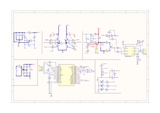
Hello! I am currently working in a design with BQ25756E but the chip dosen't work.Currently our chip has about 15V input to the VAC connector, and the ACUV and ACOV resistors are programmed in the range of 4.2-40V. The CE connector is connected to the ground to provide a low level, but the chip does not work properly. My questions are as follows.
1. Is it possible to dangle the SDA, SCL and INT, TS interfaces when the chip is programmed with pure resistors, because we are not using I2C?
2. Can we replace the battery with a resistor for the initial test?
3. Is the charging mode default when the chip is programmed with pure resistor? If it is the default, what is its exact operation mode?

Thanks in advance!

  • Hello,

    Thanks for working on this. What is the chip's behavior here?

    1. Yes, you can leave SDA, SCL, and INT floating. Make sure the TS pin has 3V when you are not using a thermistor.

    2. Yes, you'll need to set EN_PRECHG=0 when using a resistor as a load though. If possible, I would recommend using a constant voltage load for the BQ25756E.

    3. Yes, the BQ25756 should charge and output a current by default.

    Best Regards,
    Ethan Galloway

  • Hello,

    Thanks for your advice!Our circuit diagram is shown in the attached image, the input label in the diagram represents the input DC voltage, and in the upper right corner of the diagram we have additionally added a MOSFET discharge circuit containing the driver chip.
    In the current test we set the resistor R33 on the TS side to 1 ohm and input 3V to the TS pin, the SCL, SDA and INT pins are still left floating, but the chip is still not working properly, there is no power supply to the REGN and buck-boost circuit pins of the chip. We have input 15V to the input label, the battery is replaced by a 10V constant voltage load, which should be within the operating range of the chip according to the size of our resistor programming. But now we can only observe the light emitting diodes blinking at the PG,STAT1,STAT2 pins, and we think that the voltage at REGN here is generated by the 3V we gave to TS. We have checked the chip soldering again and it should be fine, where do you think we should modify it?
    Besides that, you mentioned that we should set EN_PRECHG=0 if we use resistive load instead of battery, do we still need to set it if we use constant voltage load?
    Thanks in advance!

  • Hello,

    Thanks for sending the schematic. I have a few questions/suggestions for the schematic:

    • Can you send me the data sheets for the FETs, inductors, and BTST diodes?
    • Make sure the BTST diodes are schottky diodes
    •  Can you short R30?
    Besides that, you mentioned that we should set EN_PRECHG=0 if we use resistive load instead of battery, do we still need to set it if we use constant voltage load?

    No, you don't need to set EN_PRECHG=0 if you use a constant voltage load.

    We have checked the chip soldering again and it should be fine, where do you think we should modify it?

    I would make sure the that the BTST diodes are schottky diodes and make sure that the VGS(th) of the FETs is around or below 2V. |

    Can you also measure the output of VBAT, SW1, SW2 and REGN with an oscilloscope.

    If possible, I would also recommend reading the I2C status and flag register to see what the IC's status is.

    Best Regards,
    Ethan Galloway

  • 你好

    感谢您的回复!The data sheets for the BTST diodes are shown in the attached file.We use the same schottky diodes V1FM10-M3/H as

    shown in BQ25756EVM.

    10A8167CE7140B0A2EB8D1D8CF2A1F11.pdf

    As for FETs,we select  IPD053N08N3GATMA1 whose minimum VGS(th) is 2V.I can't upload data sheets of the FETS and inductor

    successfully so I make screenshots as follows:

    FETS:

    inductor in the DC-DC module:

    As for inductor L1,I made a flat coil for my WPT system and I havn't used it yet since I input DC voltage at input label.

    I'll short R30 and test again later.And I measured the output of VBAT, SW1, SW2 and REGN with an oscilloscope yesterday but I can't see any output wave

    of these pins generated by the chips.I can only observe REGN at 3V when we input 3V DC voltage at TS pin.

    Regarding your recommendation to read the I2C registers to observe the chip status, we are currently working on it. However, since we are not familiar with

    I2C programming, we have the following questions:

    1. We have connected pin header at INT, SDA, SCL pins, do we just need to add a transfer interface similar to EV2400 to program I2C in the computer?

    2. We only want to accomplish simple one-way charging, so could you please provide the relevant sample programming code?

    Thanks in advance!


  • Hello,

    Thanks for the new information.

    I'm looking at the FET datasheet and I see that the typical VGS(th) is 2.8V with a maximum of 3.5V. Can you increase the voltage supply on DRV_SUP to see if the charger works then? Make sure to disconnect DRV_SUP from REGN when you do this. You can also try to use FETs with a lower VGS(th).

    Can you also use an oscilloscope to measure the input voltage and make sure the input voltage is good?

    1. Yes, an interface like the EV2400 or USB2ANY would help to program the IC or read the registers.

    2. Here's the driver for the IC: BQ25750_FreeRTOs_Driver.zip. This driver should allow you to use an external microcontroller to read or write to the BQ25750.

    Let me know if this makes sense and let me know if you have any questions about this.

    Best Regards,
    Ethan Galloway

  • Hello,

    Thanks for your advice!We will test again according to your reply.

    Can you also use an oscilloscope to measure the input voltage and make sure the input voltage is good?

    Yes,we have done this befor and the input voltage is good.

    Before we test again,we have some questions for resistor and I2C programming:

     resistor programming:

    1.Since we input 3V DC to the TS pin as you suggested earlier, should we disconnect resistor R23 between REGN and the TS pin in the upper right

    corner of the schematic we sent earlier?

    2.What abnormal state is represented by the light-emitting diodes connected to STAT1, STAT2, and PG blinking instead of being permanently on or off?

    I2C programming:

    1.We found in EVM User's Guide: BQ25756EVM file that the INT pin is not connected to bqstudio via EV2400, may we know how to set the INT pin when using EV2400 for I2C programming with bqstudio?

    2.If we use a microcontroller for I2C programming, do we just need to connect the SCL and SDA pins to the microcontroller via the USB-I2C interface?

    Thanks in advance!

  • Hello,

    Resistor programming:

    1. Yes, you can do this. Just make sure to use a 3V DC source or 3V from a resistor voltage divider.

    2. Do you have a battery connected in this configuration? I can think of a few scenarios that might cause this:

    • Scenario 1 - No battery or no load: The BQ25756E is charging the output capacitors and then reaching the termination current. When the VBAT capacitor voltage falls, the BQ25756E goes into recharge mode and starts the process again.
    • Scenario 2 - With a battery or load: The BQ25756E is pulling too much current from the input supply causing the power to brown out. The input supply then comes back up and the BQ25756E starts trying to charge again. You've already measured the input voltage with an oscilloscope so I think this is unlikely.

    I2C programming:

    1. You don't need to connect the /INT pin. The /INT pin is mainly used for a microcontroller to indicate that the the BQ25756E has changed statuses. The /INT pin is optional.

    2. You can connect the SDA and SCL at either J4 or J5. You can also connect at TP33 and TP34.

    Let me know if you have any questions about this.

    Best Regards,
    Ethan Galloway

  • Hello,

    Thanks for your advice,recently we have made some progress,now I would like to ask if both VAC pins(33 and 32) of the BQ25756 chip need to be connected together if  the chip is only used for positively charging for only resistor programming?

    Thanks in advance!

  • Hello,

    Yes, both VAC pins will need to be connected together.

    Best Regards,
    Ethan Galloway