This thread has been locked.

If you have a related question, please click the "Ask a related question" button in the top right corner. The newly created question will be automatically linked to this question.

BQ2970: Leakage current

Part Number: BQ2970

Tool/software:

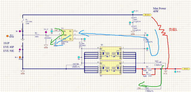
The customer is concerned that there will be leakage current in the below two circuit loop under over current protection and under voltage protection.

Could you help to comment on this?

Blue one  (B+)P+--Load--P negative--R7--R5--CO--VSS--B-

Green P+--Load--P Negative--VM--VSS--B-

  • For the green one , what is the equivalent internal resistance between VM (V-)--VSS?

  • Hello Fabio,

    During under voltage protection, the V- pin is internally pulled up to the BAT by the resistor Rv-d. The current sink, Iv-s, is not active in this state, and if there was any ‘leakage’, it would go towards BAT instead of the VSS.

    For overcurrent:
    1) Discharge Overcurrent: The V- and VSS pins are connected by a constant current sink (Iv-s) which is used to detect a load.

    2) Charge Overcurrent: The resistance Rv-d between V- and BAT and the current sink Iv-s is not connected.

    More detail is given in Section 8.4.3 Over-Discharge Status, 8.4.4 Discharge Overcurrent Status (Discharge Overcurrent, Load Short-Circuit), and 8.4.5 Charge Overcurrent Status of the datasheet

    Best Regards,
    Alexis

  • For overcurrent:
    1) Discharge Overcurrent: The V- and VSS pins are connected by a constant current sink (Iv-s) which is used to detect a load.
    -- So during an OCD situation, if the load is not removed, there will be a leakage.The range of the leakage current can be referred to the specification as "Current sink on V-", which is 8-24μA?
    2)It mentions that when CO and DO are turned off, there is still a threshold voltage of 0.5V. Is this 0.5V threshold measured relative to VSS for both the CO level and the DO level? Please refer to Section 6.5 DC Characteristics -- FET Output, DOUT and COUT for the description of VOL.

  • Hello Jian,

    1) I wouldn’t call it leakage current, however, due to the current sink, you can expect around 8 to 24uA to be pulled. Once the load is removed, the V- pin goes to VSS(BAT/2) potential. This is stated in Section 8.4.4 Discharge Overcurrent Status (Discharge Overcurrent, Load Short-Circuit) of the datasheet.

    2) The COUT pin should be respect to V-, and the DOUT pin should be with respect to VSS. This is mentioned in Section 7.2 Test Circuits of the datasheet.

    Best Regards,
    Alexis

  • The statement that "the COUT pin should be with respect to V-" was not found in sections 7.2 & 7.3. However, the 8.2 Functional Block Diagram shows that COUT is pulled down with reference to VSS, not V-. Please help to confirm this.

  • Hello Jian,

    The Functional Block Diagram shows a simplified version of the internals of the circuit.

    The COUT pin connects to Pack-/V- pin when the FET is turned OFF. Section 7.2 Test Circuits mentions it here in the image below:


    You can also refer to Section 5.1.5 Charge FET Gate Drive Output: COUT in the datasheet.

    Best Regards,
    Alexis

  • Hello Jian,

    After reviewing this post some more, I realized there might have been some confusion between what was asked and my reply.

    To clarify:
    1) The COUT pin is pulled internally to VSS when the COUT pin is turning OFF the CHG FET after detecting a fault. This is correctly shown in the Functional Block Diagram.
    2) However, when measuring the voltage at the COUT pin, due to the CHG FET, now being OFF, the COUT pin should be with respect to V-/PACK-.

    I apologize for any confusion this may have caused.

    Best Regards,
    Alexis