Tool/software:
The layout guidelines for the TPS2490 provide the following:
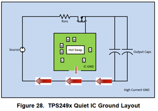
"The ground connection for the various components around the TPS2490 must be connected directly to each
other and to the TPS2490's GND pin, and then connected to the system ground at one point. Do not connect
the various component grounds to each other through the high current ground line."
and then the graphic:
I can safely assume this applies to the ground connections for Vref/PROG bias resistors and the timer capacitor, and probably even the enable pin UVLO input resistors, but what about:
- Vcc bypass capacitor
- RC circuit connected to the GATE pin for dV/dt startup
I assume I actually want the Vcc bypass capacitor grounded close to the sense resistor to keep that loop area small. For the RC circuit I'm not sure.
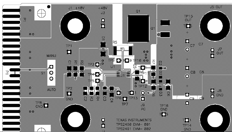
I checked the eval board layout for reference but it does not appear to follow this guidance at all. Everything is connected to a large top side ground pour: