This thread has been locked.

If you have a related question, please click the "Ask a related question" button in the top right corner. The newly created question will be automatically linked to this question.

LM5123-Q1: About the burn near pin 7 (HB terminal)

Part Number: LM5123-Q1
Other Parts Discussed in Thread: LM5123EVM-BST

Tool/software:

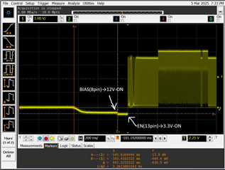
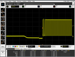
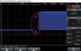
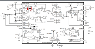
Hello I need an answer urgently. I am designing a boost converter circuit (Vin 7-32V, Vout 15-43V) using LM5123.

In the circuit I designed, burnout has occurred at pin 7 (HB terminal) in a specific location or in the test environment.

Could you tell me what could be the cause of this?

  • Hello Katsuki,

    Most likely one of the Absolute Maximum Ratings has been violated (see chapter 7.1 of the datasheet).

    Please note that the pin where you can see the damage need not be the one that has seen the overstress.
    It is normal that the damage which appears as a consequence of an over- or undervoltage stress will happen at some completely different pin.
    Any violation of the Absolute Maximum Ratings, even if it only happens for a short Periode of time kann degrade of even damage the part.

    If you want to concentrate on the HB pin first, the typical scenario which causes a violation of the voltage ratings is a big ringing, especially undershoots of the switch node.
    In that case, the capacitor between HB and SW will get charged to a voltage which is higher than the allowed maximum, which will cause overstress on the HB pin.

    You may try to use gate resistors of up to 5 Ohms (please make sure that both resistors will always have the same value).
    Or you can try different FETs which are switching slower to minimize the ringing on the switch node.

    Best regards
    Harry

  • Hello Harry,

    Thank you for your reply.
    I'll check again if you don't violate any of the posts.

    About SW node undershoot, confirmed.
    When the gate resistance is 0Ω, the resistance is about 2~3V.
    As you said, I thought it might have caused overvoltage and stress to the HB terminal due to the undershoot.

    That's why we talk about gate resistance values.
    The reason why the gate resistance is 5Ω is the maximum.
    If the gate resistance is increased, the switching loss will increase, but is there any other reason?
    Please tell me to examine the appropriate value of gate resistance value.

     Best regards
    Katsuki

  • Hello Katsuki,

    Higher gate resistors will make the transitions of the FETs more flat.
    The dead-time of the LM5123 is only 20 ns.
    The device is using an adaptive dead-time control (break before make concept), but it can only see the signals on its own pins and not the signals behind the gate resistor at the gates of the FETs.
    When the gate resistors are too big, it may happen that there is a cross-conduction where one FET already turns on while the other one has not yet fully turned off.

    You can try using a snubber in addition to reduce the ringing of the switch node.
    Or - as mentioned before - different FETs which are switching slower.

    Best regards
    Harry

  • Hello Harry,

    We are considering this, but the same damage occurred even when the gate resistance was set to 3.3 Ω. We believe that undershoot of the SW terminal may not be the direct cause.

    We are using the LM5123 with the SYNC and TRK pins connected to an audio IC (TAS6584QPHDRQ1). Is it OK to use it in a synchronous configuration when connecting it to the TAS6584QPHDRQ1?

    Are there any other points to note when connecting it to the TAS6584QPHDRQ1?

    We are considering changing from a synchronous type to an asynchronous type using a diode, although we are not sure if this will solve the problem. What do you think?

    Best regards
    Katsuki

  • Hello Katsuki,

    As you can see from the datasheet, there is not much margin for the undershoot of the switch node and the HB voltage.

    I am not certain if the word "synchronous" is used with two different meanings here.

    Connecting the sync pin and the TRK pin is o.k. So both parts will run synchronously with the same frequency.

    An Asynchronous controller with a diode instead of the high-side FET is not recommended for a higher power application like an audio amplifier
    and would destroy all the power savings that you gain with the class-H concept.

    Please have a look at our class-H reference design, based on the LM5123:
    https://www.ti.com/tool/TIDA-020033 


    All information in this correspondence and in any related correspondence is provided “AS IS” and “with all faults” and is subject to TI’s Important Notice: http://www.ti.com/corp/docs/legal/important-notice.shtml 


    Best regards
    Harry

  • Hello Harry,
    As you say, there is not much margin for switch node undershoot and HB voltage, and even if measures such as base resistors and snubber circuits are implemented, it is difficult to keep the voltage within 5.8V while taking into account variations. As a result, we are considering changing to an asynchronous system, although the efficiency will decrease. If we change to an asynchronous system, are there any disadvantages other than the efficiency?

  • Hello Katsuki,

    I never stated that the HB pin is the one that has suffered from overstress.

    Please let me repeat that the pin where you can see the damage need not be the one that has seen the overstress.
    It is normal that the damage which appears as a consequence of an over- or undervoltage stress will happen at some completely different pin.

    So, please double-check all other pins as well.


    As far as I am aware, we do not have any asynchronous controller with Track pin.
    To connect an external feedback divider to the control-signal of the audio amplifier, you will need to invert the direction of that signal.


    Best regards
    Harry.

  • Hello Harry,

    I have checked the waveforms of each pin of the LM5123, and so far there are no waveforms that exceed the maximum rating.

    I am checking the waveforms of each pin of the LM5123, and so far there are no waveforms that exceed the maximum rating. When I tried to measure the voltage between HB and AGND, the IC failed and the input voltage started to appear directly in the output voltage. Could the failure be caused by the capacitance of the probe used during measurement, etc.?

    Best regards
    Katsuki


  • Hello Katsuki,

    I have never heard of such a case.

    It would need to be a very bad (or maybe broken) probe with a huge capacitance.

    One of these reasons seems to be more likely to cause a damage of the controller:
    - The HB pin was probed with a direct 50 Ohm input of the oscilloscope
    - The HB pin got shorted to the adjacent BIAS pin (even if it was only for a very short period of time)
    - Mechanical force on the package of the controller caused some effect due to issues with the solder joints (e.g. underneath the IC)

    Best regards
    Harry.

  • Hello Harry,

    I measured between the HB(+) and SW(-) terminals with a differential probe.
    I have attached the waveform.

    The waveform between the terminals has a negative potential before oscillation begins.
    Is this normal behavior? What causes this behavior?
    The measured output voltage of the IC is normal.

    The timing when 12V was applied to the BIAS pin
    and the timing when 3.3V was applied to the EN pin have been added to the waveform.

    Best regards
    Katsuki.

  • Hello Harry,

    Is the behavior of the waveform circled in red in the attached waveform normal?

    Also, what could be the cause of this?
    Please let me know the possible causes.

    Best regards
    Katsuki.

  • Hello Katsuki,

    Did I understand correctly that the yellow signal is the voltage across the HB capacitor (from HB to SW)?
    It should not be switching so much.
    Maybe you can show me a zoomed in version which just shows a few cycles.

    Maybe you need to use a different capacitor on the HB pin.
    It needs to act as an cycle-by-cycle energy storage for the high-side gate-driver.
    This capacitor needs to be low ESR, low ESL, and have a very low leakage. Also, considering the DC BIAS effect, please choose a capacitor with a high nominal voltage.

    Why are there two different voltage levels in the upper image (with these two short drops)?
    What is going on there?


    What is the blue signal?
    Is it also the HB vs. SW voltage?

    Can you please show the VCC vs. GND voltage in parallel / in one screenshot?

    Thanks,
    Harry

  • Hello Harry,

    >Why are there two different voltage levels in the upper
    >image (with these two short drops)?
    >What is going on there?
    We would like to know the reason for this.
    Is there anything you can predict?

    The timing of the two drops occurs when the BIAS power supply
    is turned on and when voltage is applied to the EN terminal,
    as shown in the first waveform.

    Let's try adjusting the capacitance of the capacitor on the HB pin.


    The blue signal shows the waveform between the HB(+) terminal and the SW(-) terminal.
    I will also capture and send the waveform between VCC (pin 9) and GND.

    Best regards
    Katsuki.

  • Hello Harry,

    There is a diode in the path supplying VCC to the high-side gate driver.
    What is the leakage current that flows in the reverse direction through this diode?

    Best regards
    Katsuki.

  • Hello Katsuki,

    I am really confused by your description about the two drops. The BIAS and EN events are happening much earlier ...

    Anyway, that diode from VCC to HB is integrated into our device.
    Do not use an external diode in addition!
    An external diode would cause issues.

    If I misunderstood, what else do you mean with "There is a diode in the path supplying VCC to the high-side gate driver."?

    Best regards,
    Harry

  • Hello Harry,

    Sorry, I forgot to attach the image.

    This is the diode inside the IC shown in the image.

    Best regards
    Katsuki.


  • Hello Harry,

    I checked the voltage at startup on your evaluation board (LM5123EVM-BST).
    The waveform was acquired with a differential probe.
    The blue line is the voltage between the HB (+) and SW (-) terminals.
    The green line is the voltage between VCC (+) and GND (-).

    Just like the waveform measured on our board, a potential of -0.59V is displayed
    before oscillation begins.
    Does this mean the device is operating normally?
    Also, what causes this?
    Please let me know.

    Best regards
    Katsuki.

  • Hello Katsuki,

    The negative voltage on the HB pin BEFORE the first switching of the FETs is normal.
    The HB capacitor will only be charged (with a positive voltage) when the low-side FET is turns on for the first time.

    Elder devices often required an external diode and customers ran into issues because some wrong diode was chosen.
    So, we decided to integrate it into the controller to make sure that it will switch fast enough and has very low leakage.

    The voltages (VCC and HB) in your screenshot are vey low. Basically too low for a proper operation.
    VCC should usually be regulated (down) to 5V.
    When the BIAS voltage is bigger than 3.8V, the controller will start working.
    But it can not generate 5V on the VCC pin and the HB voltage will be even lower (3.75V in your measurement).

    So I would believe that in your setup the BIAS voltage is just around 4.2V.

    With such low voltages it is not guaranteed that the FETs are switching properly.
    Also, the timing of the FETs can be different than expected and you may encounter false turn on / turn off events going on.
    Worst case this may even lead to cross-conduction between the two FETs.

    Therefore, please increase the BIAS voltage in your system.
    Either make sure that the input voltage will not fall below 5.5V

    Or connect the BIAS pin to VOUT instead of VIN.
    For startup, VIN will go across the body diode of the high-side FET to VOUT and also to BIAS, so it has to be around 4.5V .. 5V to allow for the controller to start up.
    But when the input voltage drops afterwards, the controller will be supplied by the self-boosted output voltage.

    This discussion just reminds me of another problem which can occur with a lab setup and which might cause your original issue:
    If the lab supply for VIN is running into a current limit it may happen that the boost converter cannot deliver the required energy to the output.
    It will also not go into any protective mode as there will never be an overcurrent happening.

    This constellation can also damage a converter stage.

    So, please make sure that the lab supply will always deliver the required peak inductor current plus same margin.

    Best regards
    Harry

  • Hello Harry,

    I believe the voltage between HB and SW depends on VCC and the Vf of the internal diode,
    but could you tell me how much it varies at a constant temperature (for example, Ta = 25°C)?


    Also, could you tell me how much the voltage between HB and SW varies with temperature?

    If you have any measurement data, please send it to me.

    Best regards
    Katsuki.

  • Hello Katsuki,

    > I believe the voltage between HB and SW depends on VCC and the Vf of the internal diode,
    This is correct.

    > could you tell me how much it varies at a constant temperature (for example, Ta = 25°C)?
    1) When the BIAS voltage is high enough, so that the VCC regulator is enabled, the VCC voltage falls between min=4.75V, typ=5V, max=5.25V

    2) When BIAS is less than the 5-V VCC regulation target (VVCC-REG), the VCC output tracks the BIAS pin voltage with a small dropout voltage
    which is caused by 1.7-Ω resistance of the VCC regulator.
    For the Minimum supply voltage VBIAS=3.8V and the maximum load current on the VCC pin IVCC=100mA The minimum VCC voltage is specified as 3.45V.

    The VCC voltage will then go across the internal diode, with a HB diode resistance of typically 1.2Ω

    Typical values correspond to TJ = 25°C.
    Minimum and maximum limits apply over TJ = –40°C to 125°C, unless otherwise stated.

    > could you tell me how much the voltage between HB and SW varies with temperature?
    - While the regulator is active, VCC varies across temperature from min=4.75V to max=5.25V
    - For the HB diode resistance, the datasheet only mentions a typical value of 1.2Ω. So, I would consider about 25% tolerance to the diode resistance.

    > If you have any measurement data, please send it to me.
    I am sorry, but for parameters which are not listed in the datasheet, we do not capture any data during ATE tests.
    If I did take measurements on a single board/device, it would not be representative at all, so I will not spend any time on that.

    Best regards,
    Harry

  • Hello Harry,

    The maximum rating between HB and SW is -0.3 to 5.8V (5.5V),
    but the VCC voltage is a maximum of 5.25V,
    so there is little margin and I am having difficulty with the design.
    Are there any countermeasures to this?

    Also, I understand that the negative voltage on the HB pin before the initial switching start is normal,
    but could you tell me why this is normal?


    Best regards
    Katsuki.

  • Hello Katsuki,

    The only realistic countermeasure is to keep the undershoots on the switchnode as small as possible.

    Any pre-charged voltage of the HB capacitor will be clipped by an internal diode
    Anyway, it is normal and will not harm the device.

    All information in this correspondence and in any related correspondence is provided “AS IS” and “with all faults” and is subject to TI’s Important Notice: www.ti.com/.../important-notice.shtml

    Best regards
    Harry

  • Hello Harry,

    To prevent undershoot of the switch node,
    have you adjusted the gate resistance and the capacitance of the capacitor between SW and HB correctly?

    Also, the voltage difference between HB and SW is steadily around 5.5V,
    and I am concerned that this may exceed the maximum rating due to noise, etc.
    Are there any measures to be taken in this regard?


    Best regards
    Katsuki.

  • Hello Katsuki,

    The capacitance of the capacitor between SW and HB must not be changed.
    Please make sure, that you are using low ESL, low ESR type capacitors.

    The best resistance for the gate resistors needs to be determined by experiments and measurements on the physical PCB in the lab.
    You can also place a snubber in parallel to the FET.

    Most importantly, a good layout with very small parasitics in the power path (especially from the low side FET to PGND) and the gate loops is mandatory.

    Again:
    The only countermeasure is to keep the undershoots on the switchnode as small as possible.
    Everything else (VCC voltage, diode drop) is fixed within the controller.


    To be honest, you are the only customer who is so much worried about the HB voltage.
    A steady level within the specification is fine and short spikes due to noise are tolerable.

    Best regards
    Harry