This thread has been locked.

If you have a related question, please click the "Ask a related question" button in the top right corner. The newly created question will be automatically linked to this question.

LM5148: Absolute maximum rating of <20ns

Part Number: LM5148

Tool/software:

Hi,

The absolute maximum ratings list a relaxed specification of <20ns.

Is this because the LM5148's deadtime is 20ns (typ.)?

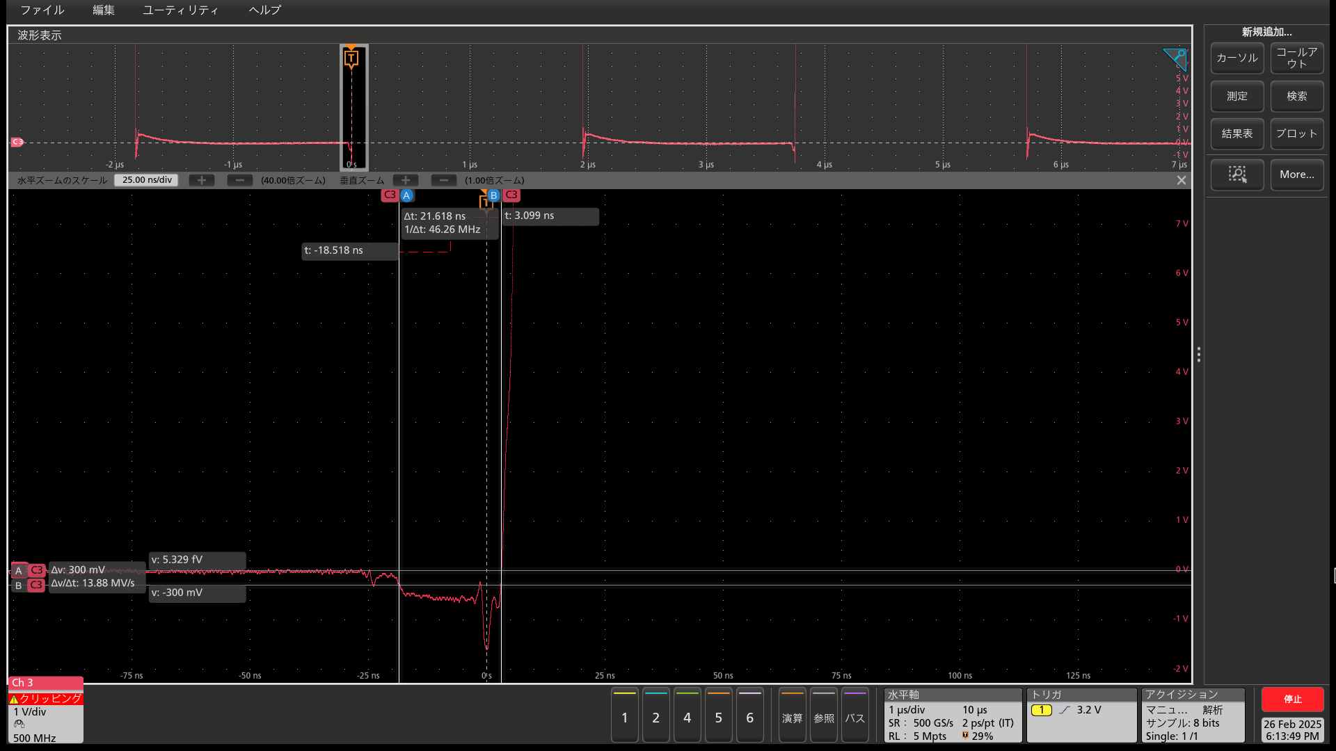
The figure below shows the waveform at the SW terminal.

The time it falls below -0.3V is more than 20ns, so it does not meet the absolute maximum rating.

I think this is because it was evaluated using an individual with a deadtime of around 22ns, but can we assume that there is no problem if it exceeds 20ns slightly?

Best regards,

  • Hello,


    No, not because of the deadtime.  The device has been rated to withstand this amount of electrical stress stated as a max voltage over time.  Need to make sure you do not violate this specification.  Check how you are measuring this, needs to be measured with tip and barrell method, with the scope probe right by the device.  if you are grossly violating this specification, it may be due to layout.

    Hope this helps.


    David.

  • Hi,

    Of cource, the measurements are used with tip and barrel method.

    I confirmed that the SW terminal voltage adheres to the absolute maximum rating.

    The measurement conditions are

    ・Using LM5148 to design a 48V input, 24V output circuit with dual-phase, PFM setting.

    ・the attached file shows the waveform when the output current is 1A and 10A.

    While the inductor current flows through the body diode of the low-side FET, the SW terminal voltage exceeds -0.3V,

    and the time that it exceeds -0.3V is at least tdead2 (LO off to HO on deadtime),

    and in discontinuous current mode at light loads, the time period is longer than this.

    lm5148_Absolute-maximum-rating-of-20ns.pdf

    I think the reason it exceeds 20ns is not due to layout.

    it's unavoidable due to the operating principle, and what do you think?

    Best regards,

  • Hello 

    Can you confirm this was measured at the device and not the FETs.  Also, it will really depend on the FETs you are using.

    Hope this helps.

    David.

  • Hi,

    Of course, the measurements are taken at a point very close to the SW terminal of the IC.

    When you say it depends on the FET, does that mean it depends on the Vf of the body diode of the low-side FET, and must select a FET with a Vf of 0.3V or less?

    Or does it mean that if you choose the right FET, the time to exceed -0.3V will be within 20ns?

    Best regards,

  • Hi,

    I measured the SW waveform with the LM5149-EVM, but the waveform was the same as that of the board I created, which does not meet the absolute maximum ratings.

    The EVM measurement waveform has been added to the file.

    lm5148_Absolute-maximum-rating-of-20ns_02.pdf

    The required value is <20ns, but it exceeds it by nearly 200ns. Does it really meet the absolute maximum rating?

    Best regards,

  • Hello,

    I suspect it a measurement error, without a photo of how you are measuring it and the probes you are measuring it with, it's really hard to say.  I will need to get into the lab and check this.  I will get back to you early next week. 

    Thanks for your patience.

    David. 

  • Hi,

    How is the progress?

    Will it take some time to get a response?

    Best regards,

  • Hello,

    Let me take a look tomorrow, sorry for the delay.

    David

  • Hello 

    I took the scope shots.  You can see its not as bad as the images you sent me.  This was taking on the SW falling, which is the worst case, rising edge shows very benign waveforms not even close to violating the -0.3V spec.  Please also note: the -0.3V is a DC specification not a switching one, so even the waveforms you took are OK.

    Here is what I took, you can see the DTs is less than 20ns.  and it quickly goes above the -0.3V specification.  Again, I think these waveforms are acceptable.  

    Hope this helps.

    David,

  • Hi,

    I don't understand why this waveform is OK, so please explain.

    【Question1】

    Is the 19ns period of your measured waveform tdead1 (HO off to LO on deadtime)?

    【Question2】

    The 20ns for tdead1 and tdead2 is a typical spec, and there should be some units that exceed 20ns.

    That unit cannot apply transient<20ns and cannot comply with the absolute maximum rating. How should I think about this?

    【Question3】

    The period when it exceeds -0.3V is 122ns. If it is within 20ns it will be relaxed to -5V, but that cannot be applied.

    I don't understand why this is OK, so please tell me the details.

    【Question4】

    Please also show us the SW waveform when the load is light and the inductor current is discontinuous.

    When the inductor current is flowing through the body diode of the low-side FET, does it exceed -0.3V and is the duration long?

    Best regards,

  • Hello,


    Question 1. Yes.

    Question 2. I will need to get some information from product Engineering and get back to you.

    Question 3. As mentioned, the -0.3V is a DC specification.  Our measurement is not pure.  We have shipped millions of these products without any issue.

    Question 4.  Will need to get back to you.

    David.

  • Hello,

    Discussed internally and we all agree of the following.

    1. As mentioned, the -0.3V is a DC specification and should not be assumed to be a risk if you go beyond this during short switching events. Said another way the -0.3V DC specification is not being violated in the waveforms you have provided above.  The minus 5V in 20ns is more of a meaningful specification here, to consider.
    2. For the purpose of safety during transients you can assume that the spec can be interpolated from -5/20ns to -0.3V/DC. even if there is a nonlinear relationship going to -0.6V in 500ns is not going to put the device at risk of failure.


    Clearly, we have work to do on the electrical table which we are discussing internally to get fixed and provide more concrete guidance, as in your case, for future consideration.


    As mentioned, your waveforms do not pose a risk to our device.  this is the best I can do with the information I currently have.


    Thanks.


    David.

  • Hi,

    This is a graph where three points, -5V@transient<20ns, -0.6V@transient<500ns, and -0.3V@DC, are linearly interpolated.

    Can we assume that there is no problem if these conditions are met?

    I have also plotted the measured value, and there is quite a bit of margin.

    Best regards,

  • Hello,

    I confirm, and as mentioned previously, I do not see your measured values posted as a risk of device damage.

    I hope this helps,

    David.

  • Hi,

    Thank you.

    So we will proceed with the circuit design using the above diagram as the maximum rating for derating the SW terminal.

    Best regards,

  • Sounds good, thank you.

    David.