This thread has been locked.

If you have a related question, please click the "Ask a related question" button in the top right corner. The newly created question will be automatically linked to this question.

LM74910-Q1: Clarification is required regarding TVS diode selection

Part Number: LM74910-Q1
Other Parts Discussed in Thread: TVS3300, TVS1800

Tool/software:

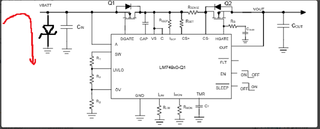
In the LM74910-Q1 datasheet, page 32, paragraph 10.2.4 MOSFET Selection: Blocking MOSFET Q1 the following statement confusis me:

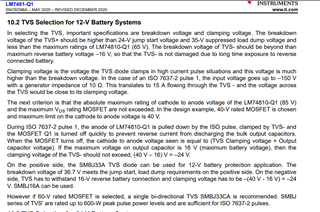
"It is recommended to use MOSFETs with VDS voltage rating of 60 V along with a single bidirectional TVS or a VDS rating 40-V maximum rating along with two unidirectional TVS connected back-back at the input. "

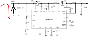
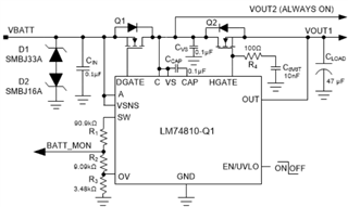
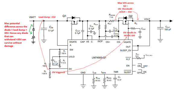
We have a 12V dual battery system and want to use active ORing using two LM74910-Q1 devices.

Since we are looking for very high current (115A) with a single MOSFET solution with RDS(ON) < 0.5mOhm, 40V VDS seems to be a better choise and IAUCN04S7N004 seems to be a good option (VGS=20V).

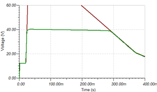
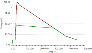
We were thinking to use a single bidirectional TVS, e.g., TPSMC22CA-VR w. 1500W having max. clamping voltage of 35.5V @42.3A (Vc@125*C = Vc@25*C x (1+0.092/100 x (125*C-25*C))=38.76V) and reverse stand-off voltage of 22V @1uA max. in both directions.

Eventually, to provide more margin, we may choose TPSMC20CA-VR having max. clamping voltage of 32.4V @46.33A (Vc@125*C = Vc@25*C x (1+0.091/100 x (125*C-25*C))=35.35V) and reverse stand-off voltage of 20V @1uA max. in both directions.

Note: The SMBJ series proposed in your datasheet (10.4.2 TVS Selection for 12-V Battery Systems) has very large interval between reverse stand-off and max. clamp voltage. For example, SMBJ18CA with VRM=18V  vs. Vc=39.3V@25*C / 42.9V@125*C.

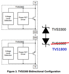
However, your datasheet proposes to use two unidirectional TVS connected back-to-back for VDS=40V.

Why? Why is this better than a bidirectional TVS? What am I missing in my understanding of TVS diodes?

Your application note "How to select a Surge Diode" (www.ti.com/.../slvae37.pdf also confuses me when it comes to dynamic resistance to be counted in the clamping voltage.

The TVS datasheet does not provide any data for the dynamic resistance. I assume that the provided max. clamp voltage in the datasheet already counts the intrinsec RDYN.

Am I wrong in this assumption?

Regards,

Ferenc

  • Hi Ferenc,

    Please refer to this section for TVS selection for 40V rated FETs

    LM7481-Q1 Ideal Diode Controller with Active Rectification and Load Dump Protection datasheet (Rev. A)

    Actually, we dont use a TVS for positive side clamping. It is present just to block the power path. Otherwise, power source is just shorted to ground via TVS-.

    Actual clamping is required only at negative side as the transients in automotive violate the abs-min rating.

    Regards,

    Shiven Dhir

  • Hi Shiven,

    Thank you for your fast response.

    I do not understand why there is no need for positive voltage clamp, since in ISO 7637-2 we have pulse test 2a, 3b, and 5a that have positive spikes up to +75V at least?

    On the other hand, from the datasheet that you referred, at least I understand now why we need two unidirectional TVS back-2-back (instead of one bidirecational) for a MOSFET w. VDS=40V. The reason is, that these unidirectional TVS diodes are not identical, they are different (having different characteristics) as shown in the figure below:

    However, what I still do not understand that why SMBJ33A is chosen for the positive side with breakdown voltage of 36.7V min, 38.6V typ. @25*C which could increase to 42.46V @125*C?

    Could you elaborate on that?

  • Hi Ferenc,

    Other than load dump pulse 5A, all the pulses are low on energy, and we rely on input and output capacitors to suppress them. Due to which controller remains safe. Pulse 5A is high in energy and TVS may not be able to clamp it (unless very strong TVS used). Hence, we use a special common source topology shown in datasheet to tackle that which uses OV pin of the controller to protect downstream load.

    SMBJ33A is chosen on positive side because a suppressed load dump pulse is of 35V in a 12V automotive system and TVS will not breakdown and try to clamp it. Controller is rated for 65V so it should be okay. If downstream load needs to be protected, we can use the OV pin.

    Regards,

    Shiven Dhir

  • Thanks for the quick replies.

  • Due to price reason and targeting very low RDS(ON), we would like to use a MOSFET w. 40V. However, it seems that the TVS diode, like SMBJ33A, is not an option for us for the above mentioned reasons. What about using TVS3300 instead?

  • Hi Ferenc,

    TVS3300 has a minimum breakdown voltage of 34V and may try to clamp a (35V) load dump pulse.

    Regards,

    Shiven Dhir

  • Hi Shiven,

    That is correct, and even if we have TVS1800 in series back2back with forward voltage of min. 0.25V that is still 34.25V.in worst case.

    Although I have never used TINA TI, now I made a rapid learning to put up a simple simulation with load dump pulse generator using piecewise linear curve and two TVS3300 / TVS1800 device back2back, as was shown in the above diagram. Based on ISO7637-2 the internal resistance of the load dump pulse test generator is between 0.5 and 5 Ohm. Then even if I set the max. value of 5 Ohm, the voltage is slightly above 40V (max. spike around 40.1V). 

    However, if I am setting the internal resistor of the generator to 0.5 Ohm, the voltage goes up to 46-47V.

    It seems to me that if you want to comply with ISO7637-2 then there is no way to use MOSFET w. 40V VSD. Am I right, or did I missed something?

  • Hi Ferenc,

    If you want to comply with ISO7637-2, 40V rated FET can be used, there isn't an issue. If there is a trouble with TVS+ selection, you can simply add a schottky rated for > 35V so that it doesnt get damaged during load dump. As I explained, the role of TVS+ is just to block the power path.

    Regards,

    Shiven Dhir

  • Hi Shiven,

    Since I am not an expert in the automotive power supply protection design, I am very thankful for you support.

    However, I do not understand your comment regarding "If there is a trouble with TVS+ selection, you can simply add a schottky rated for > 35V".  By the word "adding" do you mean to replace the TVS+ diode with a Schottky diode or what? 

    And I assume, the Schottky diode should be also rated for inverse voltage <40V. However, I could not find any automotive Schottky diode that is in that range 35V<VR<40V, only either 35V or 40V.

    So, I am still confused about how to use VSD=40V MOSFET while complying with ISO7637-2.

    Please, help me by being more specific. 

  • Hi Ferenc,

    ISO7367-2 has quiet a lot of pulses but we try to cater only pulse 1 which is -150V(peak) transient which is high in energy as well cannot be suppressed by input and output capacitors.

    To cater that pulse, we use TVS- which clamp on the negative side to keep the controller safe and also VDS of the FET safe. For a 12V system and 40V FET, we try to clamp under (40V-16V) = 24V. For this SMBJ18A or TVS1800 works fine. I hope we are clear for this.

    Next high energy pulse is the load dump pulse which is a 35V peak for >40ms which more of a DC situation and TVS cannot clamp it. Now, to work with this and protect downstream load, we use controller's OV pin and turn-off the HGATE.

    Now as I explained earlier, the TVS+ was present just to block the power path.

    The diode/TVS+ should be rated enough to withstand and not damage. 

    Now, I am unsure why you assumed that schottky should be rated for <40V. Can you help me understand? Are we misunderstanding something?

    Also, if you don't agree with any part of my explanation, please feel free to correct me.

    Regards,

    Shiven Dhir

  • Hi Shiven,

    I realized that the whole missunderstanding between us is that we have different assumptions.

    1. My assumption was that we need to withstand 14V + 87V = 101V max. as the peak of unsuppressed load dump pulse according to Test pulse 5a, that is why I wanted to suppress the positive pulse below 40V with a TVS+ (my simulation results are based on this),

    2. while your assumption is that we already have a suppressed load dump with a peak of max. 35V (test pulse 5b).

    Since we have multiple potential customers, we thought to target for the worst case. But we need to take into account other considerations, like minimizing both the price and the unwanted power dissipation on the MOSFETs (and the lower the VDSmax, the lower the RDS(ON)). So we might switch to fulfilling only the suppressed load dump (test pulse 5b).

    Thanks for your support to have a better understanding of the situation.

    Regards,

    Ferenc

  • Hi Shiven,

    One last question regarding TVS- selection. In the page that you embedded as your first response, SMBJ16A is proposed for TVS-.

    However, when I am looking into the datasheets (see LittleFuse, STMicro, Microchip, or Nexperia), the max. clamping voltage for SMBJ16A is 26V >24V.

    Is that still OK?

    Regards,

    Ferenc

  • Hi Ferenc,

    Max clamping voltage maybe 26V. But during ISO pulse 1, it clamps under 24V as the current is lesser compared to rated current against max clamping voltage,

    Regards,

    Shiven Dhir