This thread has been locked.

If you have a related question, please click the "Ask a related question" button in the top right corner. The newly created question will be automatically linked to this question.

CSD19537Q3: Spice Model Inquiries

Part Number: CSD19537Q3
Other Parts Discussed in Thread: TINA-TI

Tool/software:

Hi E2E Elites,

I'm currently using the spice model downloaded from TI website and created a symbol inside LTSpice. 

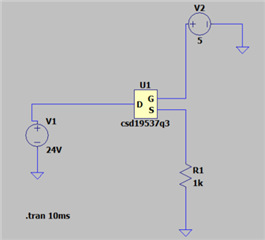
Based on the datasheet it says, Vgs needed typical 3V so that my 24V able to drop on my R1.

Below is my simulation result:

The results shown at source side is only 2V instead of 24V. 

Am I miss out anything?

Thanks.

Regards,

JS

  • Hello JS,

    Thanks for your interest in TI FETs. All of TI's 80V and 100V FETs require VGS ≥ 6V, which is the minimum value where Rds(on) is specified in the datasheet and tested in production. TI does not guarantee Rds(on) at values of VGS < 6V. The typical threshold voltage, VGS(th) specified in the datasheet is where the FET just begins to conduct (ID = 250μA). To fully enhance the FET, VGS must be driven to at least 6V. As can be seen in the Rds(on) vs. VGS graph on page 1 of the datasheet, the on resistance plot is nearly vertical at VGS = 5V.

    The simulation has the FET configured as a high side switch with the drain connected to the input voltage and the load/output voltage connected to the source. In this configuration, the gate voltage must be driven at least 6V higher than the input voltage. This is because when the FET is on, the drain and source voltages are almost equal. For the simulation to work, the gate voltage must be 30V and VGS = VG - VS = 30V - 24V = 6V. You can also change the reference for V2 from GND to teh FET source and apply 6V so VGS = 6V.

    Try using VGS = 6V (either V2 = 30V referenced to GND or V2 = 6V referenced to the source of the FET) in your simulation to see if that gives you the expected output voltage at the source of the FET. Both work when I replicate the simulation in TINA-TI. I'm including a link below to an app note on avoiding common mistakes when designing with FETs. Let me know if you have any questions.

    https://www.ti.com/lit/an/slpa021/slpa021.pdf

    Best Regards,

    John Wallace

    TI FET Applications

  • Hi JS,

    You can also use a N-channel FET as a low side switch with the load resistor connected between the input voltage and the drain with the source grounded. The gate still needs to be driven to at least 6V with respect to GND but it does not have to be higher than the input voltage.

    Thanks,

    John

  • Hi John, thanks for your help! I have understood the working principle better after your explanation.