This thread has been locked.

If you have a related question, please click the "Ask a related question" button in the top right corner. The newly created question will be automatically linked to this question.

UCC27282: the HS pin of UCC27282 is burnt out

Part Number: UCC27282

Tool/software:

Hello expert, I encountered an issue of HS pin burnout while using UCC27282 for BLDC applications
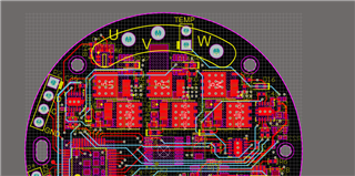
1、This is the schematic diagram I am using


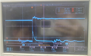
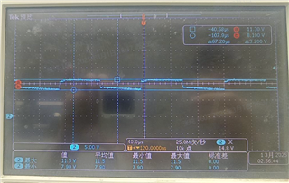
2、The motor is applied to scenarios with fast response and high load, and can instantly respond to high loads. When using a switch power supply (48V) for power supply, everything works normally; But when using a battery pack (fully charged at around 58V), the HS will burn out at the moment the motor starts, aand the accompanying MOS transistor may also break.

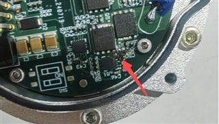
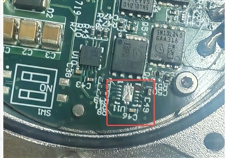
3、This is a burnt board


Looking forward to your reply very much

  • Hi Chun,


    Thank you for reaching out. I reviewed your schematic and noticed that the bootstrap capacitance on HB-HS is larger than the bypass capacitance on VDD-VSS. Since the bypass capacitor provides charge to the bootstrap capacitor, we recommend a bypass capacitance >= 10x the size of the bootstrap capacitor. Please refer to the following FAQ for more detail on bootstrap circuitry: Bootstrap Circuitry Selection for Half Bridge Configurations (Rev. A).


    Since the issue occurs the moment the motor starts, I would like to see the following scope captures:

    1. HO and HS as close to the device as possible, and Drain of the high side MOS with the 48V power supply
    2. Same pins/probe points using the 58V battery pack


    Also, what are the full operating conditions for this device? Switching frequency, duty cycle, output power?


    Thank you,

    Vincent Liew

  • Hello, expert
    1. At present, the bypass capacitor is indeed small, but the voltage across the bootstrap capacitor can fully open the MOS, so the problem may not be here. This is the relationship between the conduction voltage and current of MOS


    2. Operating conditions for gate drive chip: Input center symmetric complementary PWM, frequency 8K, for motor control
    3. The following is the waveform of the test point. Due to burning during normal use, the waveform is difficult to capture. The following waveform has a relatively slow response and the current loop is running


    The situation of 48V power supply
    Vgs (near MOS transistor), bridge up


    V (ho - hs) (near the gate driver chip)


    The situation of 60V power supply
    Vgs (near MOS transistor), bridge up


    V (ho - hs) (near the gate driver chip)

    Voltage across the bootstrap capacitor

  • Hi Chun,

    Our expert is looking at it and will get back you before EOD tomorrow. Appreciate the patience and understanding.

    Best,

    Pratik A.

  • Hi Chun,

    Thank you for the scope captures. While the voltage on the bootstrap capacitor is enough to open the MOS, I would still suggest a larger bypass capacitor just to cover all our bases.

    Would it be possible to share the layout?

    Thank you,

    Vincent Liew

  • Hello expert
    Thank you for your suggestion. We will increase the bypass capacitor

    This is the layout

    Looking forward to your reply very much

  • Hi Chun,

    The traces for HS, HO, LO, VDD, and VSS are all high current traces and should be wider and closer to the MOSFETs. Please refer to section 10 of the datasheet for more information on layout guidelines and how this impacts device operation.

    The device may be experiencing electrically induced damage. Would you be able to provide HO-HS, HS, and LO in the same scope capture with persistence turned off? Separate captures for rising and falling edge, all probed near the gate driver with high bandwidth probes.

    Thank you,

    Vincent Liew